
Datasheet


GND
LM5066
R
PG1
V
PGD
C
PG
PGD
GND
LM5066
R
PG1
Power
Good
V
PGD
C
PG
PGD
R
PG2
GND
LM5066
R
PG1
V
PGD
C
PG
PGD
R
PG2
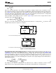
C) Short Delay at Rising Edge and
Long Delay at Falling Edge or
Equal Delays
B) Long Delay at Rising Edge,
Short Delay at Falling Edge
A) Delay at Rising Edge Only
Power
Good
Power
Good
GND
LM5066
R
PG
Power Good
V
PGD
OUT
FB
GND
PGD
GATE
UV
OV
Q1
V
OUT
R4
R5
LM5066
2.46V
20 PA
V
PGDL
= 2.46V + [R4 x (2.46V - 20 PA)]
R5
V
PGDH
=
2.46V x (R4 + R5)
R5
V
PGD(HYS)
= R4 x 20 PA
LM5066
SNVS655G –JUNE 2011–REVISED FEBRUARY 2013
www.ti.com
As an example, assume the application requires the following thresholds: V
PGDH
= 40V, and V
PGDL
= 38V.
Therefore V
PGD(HYS)
= 2V. The resistor values are:
R4 = 100 kΩ, R5 = 6.55 kΩ
When the R4 and R5 resistor values are known, the threshold voltages and hysteresis are calculated from the
following:
(35)
Figure 13. Programming the PGD Threshold
Figure 14. Power Good Output
Figure 15. Adding Delay to the Power Good Output Pin
28 Submit Documentation Feedback Copyright © 2011–2013, Texas Instruments Incorporated
Product Folder Links: LM5066