
Datasheet


UVLO
LM5026
V
PWR
1.25V
20 PA
Enable
R1
R2
0.4V
Standby
OFF
STANDBY
UVLO
LM5026
V
PWR
1.25V
20 PA
Enable Output
Drivers
R1
R2
0.4V
Enable V
CC
& V
REF
Regulators
PWR
1.25 R1
R2
V 1.25
´
=
-
HYS
V
R1
20 A
=
m
LM5026
SNVS363D –AUGUST 2005–REVISED APRIL 2013
www.ti.com
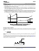
UNDER-VOLTAGE LOCKOUT (UVLO)
When the UVLO pin voltage is below 0.4V the controller is in a low current shutdown mode. When the UVLO pin
voltage is greater than 0.4V but less than 1.25V the controller is in standby mode. When the UVLO pin voltage is
greater than 1.25V the controller is fully enabled. Typically, two external resistors program the minimum
operational voltage for the power converter as shown in Figure 29. When UVLO pin voltage is above the 1.25V
threshold, an internal 20 μA current source is enabled to raise the voltage at the UVLO pin, thus providing
threshold hysteresis. Resistance values for R1 and R2 can be determined from:
where
• V
HYS
is the desired UVLO hysteresis at V
PWR
(6)
.
where
• V
PWR
is the desired turn-on voltage (7)
For example, if the LM5026 is to be enabled when V
PWR
reaches 33V, and disabled when V
PWR
is decreased to
30V, R1 calculates to 150 kΩ, and R2 calculates to 5.9 kΩ. The voltage at the UVLO pin should not exceed 6V
at any time. Be sure to check both the power and voltage rating for the selected R1 resistor.
Remote configuration of the controller’s operational modes can be accomplished with open drain device(s)
connected to the UVLO pin as shown in Figure 30.
Figure 29. Basic UVLO Configuration
Figure 30. Remote Standby and Disable Control
OSCILLATOR (RT, SYNC)
Oscillator (RT, SYNC) The oscillator frequency is generally selected in conjunction with the design of the system
magnetic components along with the volume and efficiency goals for a given power converter design. The total
RT resistance at the RT pin sets the oscillator frequency. The RT resistors should be one of the first components
placed and connected when designing the PC board. Direct, short connections to each side of the RT resistors
(RT, DCL and AGND pins) are recommended .
18 Submit Documentation Feedback Copyright © 2005–2013, Texas Instruments Incorporated
Product Folder Links: LM5026