
Datasheet


VIN
1
CS
2
SS
3
FB
4
RT
8
VCC
7
COMP
6
UVLO
5
9
10
OUT
GND
LM5022
SNVS480G –JANUARY 2007–REVISED DECEMBER 2013
www.ti.com
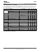
Connection Diagram
Figure 1. 10-Lead VSSOP Package
See Package Number DGS0010A
PIN DESCRIPTIONS
Pins Name Description Application Information
1 VIN Source input voltage Input to the start-up regulator. Operates from 6V to 60V.
Inverting input to the internal voltage error amplifier. The non-
2 FB Feedback pin inverting input of the error amplifier connects to a 1.25V
reference.
Error amplifier output and PWM The control loop compensation components connect between this
3 COMP
comparator input pin and the FB pin.
Output of the internal, high voltage linear This pin should be bypassed to the GND pin with a ceramic
4 VCC
regulator. capacitor.
5 OUT Output of MOSFET gate driver Connect this pin to the gate of the external MOSFET. The gate
driver has a 1A peak current capability.
6 GND System ground
Set the start-up and shutdown levels by connecting this pin to the
7 UVLO Input Under-Voltage Lock-out input voltage through a resistor divider. A 20 µA current source
provides hysteresis.
Current Sense input Input for the switch current used for current mode control and for
8 CS
current limiting.
An external resistor connected from this pin to GND sets the
Oscillator frequency adjust pin and
9 RT/SYNC oscillator frequency. This pin can also accept an AC-coupled input
synchronization input
for synchronization from an external clock.
An external capacitor placed from this pin to ground will be
10 SS Soft-start pin charged by a 10 µA current source, creating a ramp voltage to
control the regulator start-up.
These devices have limited built-in ESD protection. The leads should be shorted together or the device placed in conductive foam
during storage or handling to prevent electrostatic damage to the MOS gates.
2 Submit Documentation Feedback Copyright © 2007–2013, Texas Instruments Incorporated
Product Folder Links: LM5022