
Datasheet


Z
LEP
=
1
0.5 x (R
O
+ ESR) x C
O
Z
ZESR
=
1
R
C
x C
O
A
PS
=
(1 - D) x R
O
2 x R
SNS
ZESR RHP
PS PS
2
2
LEP n n
n
s s
1 1
G A
s s s
1 1
Q
æ ö
æ ö
+ -
ç ÷
ç ÷
w w
è ø
è ø
= ´
æ ö
æ ö
ç ÷
+ + +
ç ÷
ç ÷
w ´ w
w
è ø
è ø
+
-
+
D
+
-
+
-
V
REF
+
-
C1
C2
R1
L
C
O
R
O
V
IN
R
C
R
FB2
R
FB1
R
SNS
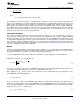
LM5022
SNVS480G –JANUARY 2007–REVISED DECEMBER 2013
www.ti.com
Figure 18. Power Stage and Error Amplifier
One popular method for selecting the compensation components is to create Bode plots of gain and phase for
the power stage and error amplifier. Combined, they make the overall bandwidth and phase margin of the
regulator easy to determine. Software tools such as Excel, MathCAD, and Matlab are useful for observing how
changes in compensation or the power stage affect system gain and phase.
The power stage in a CCM peak current mode boost converter consists of the DC gain, A
PS
, a single low
frequency pole, f
LFP
, the ESR zero, f
ZESR
, a right-half plane zero, f
RHP
, and a double pole resulting from the
sampling of the peak current. The power stage transfer function (also called the Control-to-Output transfer
function) can be written:
where
• the DC gain is defined as: (42)
where (43)
R
O
= V
O
/ I
O
(44)
The system ESR zero is:
(45)
The low frequency pole is:
(46)
The right-half plane zero is:
20 Submit Documentation Feedback Copyright © 2007–2013, Texas Instruments Incorporated
Product Folder Links: LM5022