
Datasheet


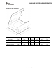

SS
COMP
+22 PA
5.2V
4.6V
-10 PA
during over
load
+22 PA
after releasing the over load
LM5021
www.ti.com
SNVS359D –MAY 2005–REVISED MARCH 2013
Figure 12. Waveform at SS and COMP Pin due to Brief Overload
SKIP CYCLE OPERATION
During light load conditions, the efficiency of the switching power supply typically drops as the losses associated
with switching and operating bias currents of the converter become a significant percentage of the power
delivered to the load. The largest component of the power loss is the switching loss associated with the gate
driver and external MOSFET gate charge. Each PWM cycle consumes a finite amout of energy as the MOSFET
is turned on and then turned off. These switching losses are proportional to the frequency of operation. The Skip
Cycle function integrated within the LM5021 controller reduces the average switching frequency to reduce
switching losses and improve efficiency during light load conditions.
When a light load condition occurs, the COMP pin voltage is reduced by the voltage feedback loop to reduce the
peak current delivered by the controller. Referring to Figure 13, the PWM comparator input tracks the COMP pin
voltage through a 1.25V level shift circuit and a 3:1 resistor divider. As the COMP pin voltage falls, the input to
the PWM comparator falls proportionately. When the PWM comparator input falls to 125mV, the Skip Cycle
comparator detects the light load condition and disables output pulses from the controller. The controller
continues to skip switching cycles until the power supply output falls and the COMP pin voltage increases to
demand more output current. The number of cycles skipped will depend on the load and the response time of the
frequency compensation network. Eventually the COMP voltage will increase when the voltage loop requires
more current to sustain the regulated output voltage. When the PWM comparator input exceeds 130mV (5mV
hysteresis), normal fixed frequency switching resumes. Typical power supply designs will produce a short burst
of output pulses followed by a long skip cycle interval. The average switching frequency in the Skip Cycle mode
can be a small fraction of the normal operating frequency of the power supply.
The skip cycle mode of operation can be disabled by adding an offset voltage to the CS pin (refer to Figure 14).
A resistive divider connected to a regulated source, injecting a 125mV offset (minimum) on the CS pin, will force
the voltage at the PWM Comparator to be greater than 125 mV, disabling the Skip Cycle Comparator.
Copyright © 2005–2013, Texas Instruments Incorporated Submit Documentation Feedback 13
Product Folder Links: LM5021