
Datasheet


ESR
(min)
=
34.5 mA
50 mV
= 1.45:
I
OR(min)
=
L1
max
x F
S(max)
x V
IN(min)
V
OUT
x (V
IN(min)
- V
OUT
)
120 PH x 201 kHz x 6V
5V x (6V - 5V)
= 34.5 mAp-p
=
C1 =
'V
I
O
x t
ON
= 13 PF
0.5V
1.0A x 6.5 Ps
=
t
ON(max)
=
6V - 1.4V
1.18 x 10
-10
x (200k + 1.4k)
+ 67 ns
x 1.25 = 6.5 Ps
I
OR(max)
=
80 PH x 154 kHz x 60V
5V x (60V - 5V)
= 372 mAp-p
I
OR(max)
=
L1
min
x F
S(min)
x V
IN(max)
V
OUT
x (V
IN(max)
- V
OUT
)
LM5010A
LM5010A-Q1
www.ti.com
SNVS376E –OCTOBER 2005–REVISED FEBRUARY 2013
This provides a minimum value for L1 - the next higher standard value (100 µH) will be used. To prevent
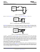
saturation, and possible destructive current levels, L1 must be rated for the peak current which occurs if the
current limit and maximum ripple current are reached simultaneously (I
PK
in Figure 10). The maximum ripple
amplitude is calculated by re-arranging Equation 12 using V
IN(max)
, F
S(min)
, and the minimum inductor value,
based on the manufacturer’s tolerance. Assume, for this exercise, the inductor’s tolerance is ±20%.
(14)
(15)
I
PK
= I
LIM
+ I
OR(max)
= 1.5A + 0.372A = 1.872A (16)
where I
LIM
is the maximum current limit threshold. At the nominal maximum load current of 1.0A, the peak
inductor current is 1.186A.
R
CL
: Since it is obvious that the lower peak of the inductor current waveform does not exceed 1.0A at maximum
load current (see Figure 11), it is not necessary to increase the current limit threshold. Therefore R
CL
is not
needed for this exercise. For applications where the lower peak exceeds 1.0A, see INCREASING THE
CURRENT LIMIT THRESHOLD.
C1: This capacitor limits the ripple voltage at VIN resulting from the source impedance of the supply feeding this
circuit, and the on/off nature of the switch current into VIN. At maximum load current, when the buck switch turns
on, the current into VIN steps up from zero to the lower peak of the inductor current waveform (I
PK-
in Figure 11),
ramps up to the peak value (I
PK+
), then drops to zero at turn-off. The average current into VIN during this on-time
is the load current. For a worst case calculation, C1 must supply this average current during the maximum on-
time. The maximum on-time is calculated at V
IN
= 6V using Equation 5, with a 25% tolerance added:
(17)
The voltage at VIN should not be allowed to drop below 5.5V in order to maintain V
CC
above its UVLO.
(18)
Normally a lower value can be used for C1 since the above calculation is a worst case calculation which
assumes the power source has a high source impedance. A quality ceramic capacitor with a low ESR should be
used for C1.
C2 and R3: Since the LM5010A requires a minimum of 25 mVp-p of ripple at the FB pin for proper operation, the
required ripple at V
OUT
is increased by R1 and R2, and is equal to:
V
RIPPLE
= 25 mVp-p x (R1 + R2)/R2 = 50 mVp-p (19)
This necessary ripple voltage is created by the inductor ripple current acting on C2’s ESR + R3. First, the
minimum ripple current, which occurs at minimum VIN, maximum inductor value, and maximum frequency, is
determined.
(20)
The minimum ESR for C2 is then equal to:
(21)
Copyright © 2005–2013, Texas Instruments Incorporated Submit Documentation Feedback 13
Product Folder Links: LM5010A LM5010A-Q1