
Datasheet


FB
SW
L1
LM5009A
R3
C2
V
OUT
R
FB2
R
FB1
SW
FB
LM5009A
L1
C2
CB
CA
RA
V
OUT
R
FB2
R
FB1
LM5009A
www.ti.com
SNVS608G –JUNE 2009–REVISED FEBRUARY 2013
where t
ON
is the maximum on-time (at minimum input voltage), and ΔV is the desired ripple amplitude at the
RA/CA junction (typically 40-50 mV). RA and CA are then chosen from standard value components to satisfy the
above product. Typically CA is 1000 pF to 5000 pF, and RA is 10 kΩ to 300 kΩ. CB is then chosen large
compared to CA, typically 0.1 µF.
Figure 16. Minimum Output Ripple Using Ripple Injection
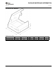
c) Alternate minimum ripple configuration: The circuit in Figure 17 is the same as that in the Block Diagram,
except the output voltage is taken from the junction of R3 and C2. The ripple at V
OUT
is determined by the
inductor’s ripple current and C2’s characteristics. However, R3 slightly degrades the load regulation. This circuit
may be suitable if the load current is fairly constant.
Figure 17. Alternate Minimum Output Ripple
Copyright © 2009–2013, Texas Instruments Incorporated Submit Documentation Feedback 15
Product Folder Links: LM5009A