
Datasheet


BST
SW
V
CC
IS
GND
LM5005
C
OUT
D1
L1
D2
V
OUT
BST
SW
V
CC
IS
GND
LM5005
V
OUT
D2
D1
L1
C
OUT
LM5005
www.ti.com
SNVS397D –SEPTEMBER 2005–REVISED MARCH 2013
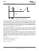
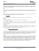
BIAS POWER DISSIPATION REDUCTION
Buck regulators operating with high input voltage can dissipate an appreciable amount of power for the bias of
the IC. The V
CC
regulator must step-down the input voltage V
IN
to a nominal V
CC
level of 7V. The large voltage
drop across the V
CC
regulator translates into a large power dissipation within the Vcc regulator. There are several
techniques that can significantly reduce this bias regulator power dissipation. Figure 20 and Figure 21 depict two
methods to bias the IC from the output voltage. In each case the internal Vcc regulator is used to initially bias the
VCC pin. After the output voltage is established, the VCC pin potential is raised above the nominal 7V regulation
level, which effectively disables the internal V
CC
regulator. The voltage applied to the VCC pin should never
exceed 14V. The V
CC
voltage should never be larger than the V
IN
voltage.
Figure 20. VCC Bias from VOUT for 8V < VOUT < 14V
Figure 21. VCC Bias with Additional Winding on the Output Inductor
Copyright © 2005–2013, Texas Instruments Incorporated Submit Documentation Feedback 19
Product Folder Links: LM5005