
Datasheet


Sample and
Hold DC Level
0.5V/A
RAMP
T
ON
t
ON
C
RAMP
(5P x (V
IN
± V
OUT
) + 25P) x
LM5005
SNVS397D –SEPTEMBER 2005–REVISED MARCH 2013
www.ti.com
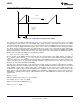
Figure 14. Composition of Current Sense Signal
The Sample and Hold DC level illustrated in Figure 14. is derived from a measurement of the re-circulating
Schottky diode anode current. The re-circulating diode anode should be connected to the IS pin. The diode
current flows through an internal current sense resistor between the IS and PGND pins. The voltage level across
the sense resistor is sampled and held just prior to the onset of the next conduction interval of the buck switch.
The diode current sensing and sample & hold provide the dc level of the reconstructed current signal. The
positive slope inductor current ramp is emulated by an external capacitor connected from the RAMP pin to AGND
and an internal voltage controlled current source. The ramp current source that emulates the inductor current is a
function of the Vin and Vout voltages per the following equation:
I
RAMP
= (5µ x (Vin – Vout)) + 25µA (2)
Proper selection of the RAMP capacitor depends upon the selected value of the output inductor. The value of
C
RAMP
can be selected from: C
RAMP
= L x 10
-5
, where L is the value of the output inductor in Henrys. With this
value, the scale factor of the emulated current ramp will be approximately equal to the scale factor of the dc level
sample and hold ( 0.5 V / A). The C
RAMP
capacitor should be located very close to the device and connected
directly to the pins of the IC (RAMP and AGND).
For duty cycles greater than 50%, peak current mode control circuits are subject to sub-harmonic oscillation.
Sub-harmonic oscillation is normally characterized by observing alternating wide and narrow pulses at the switch
node. Adding a fixed slope voltage ramp (slope compensation) to the current sense signal prevents this
oscillation. The 25µA of offset current provided from the emulated current source adds some fixed slope to the
ramp signal. In some high output voltage, high duty cycle applications, additional slope may be required. In these
applications, a pull-up resistor may be added between the V
CC
and RAMP pins to increase the ramp slope
compensation.
For V
OUT
> 7.5V:
Calculate optimal slope current, I
OS
= V
OUT
x 5µA/V.
For example, at V
OUT
= 10V, I
OS
= 50µA.
Install a resistor from the RAMP pin to V
CC
:
R
RAMP
= V
CC
/ (I
OS
- 25µA)
12 Submit Documentation Feedback Copyright © 2005–2013, Texas Instruments Incorporated
Product Folder Links: LM5005