
Datasheet


LM4936
SNAS269A –APRIL 2005–REVISED APRIL 2013
www.ti.com
The product of the desired high frequency cutoff (100kHz in this example) and the differential gain A
VD
,
determines the upper passband response limit. With A
VD
= 3 and f
H
= 100kHz, the closed-loop gain bandwidth
product (GBWP) is 300kHz. This is less than the LM4936's 3.5MHz GBWP. With this margin, the amplifier can
be used in designs that require more differential gain while avoiding performance,restricting bandwidth
limitations.
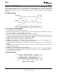
SPI TIMING DIAGRAM
SPI OPERATIONAL REQUIREMENTS
1. The maximum clock rate is 5MHz for the CLK pin.
2. CLK must remain logic-high for at least 100ns (t
CH
) after the rising edge of CLK, and CLK must remain logic-
low for at least 100ns (t
CL
) after the falling edge of CLK.
3. Data bits are written to the DATA pin with the most significant bit (MSB) first.
4. The serial data bits are sampled at the rising edge of CLK. Any transition on DATA must occur at least 50ns
(t
DS
) before the rising edge of CLK. Also, any transition on DATA must occur at least 50ns (t
DH
) after the
rising edge of CLK and stabilize before the next rising edge of CLK.
5. ENABLE should be logic-low only during serial data transmission.
6. ENABLE must be logic-low at least 50ns (t
ES
) before the first rising edge of CLK, and ENABLE has to
remain logic-low at least 50ns (t
EH
) after the eighth rising edge of CLK.
7. If ENABLE remains logic-high for more than 50ns before all 8 bits are transmitted then the data latch will be
aborted.
8. If ENABLE is logic-low for more than 8 CLK pulses then only the first 8 data bits will be latched and activated
at rising edge of eighth CLK.
9. ENABLE must remain logic-high for at least 50ns (t
EL
).
10. Coincidental rising or falling edges of CLK and ENABLE are not allowed. If CLK is to be held logic-high after
the data transmission, the falling edge of CLK must occur at least 50ns (t
CS
) before ENABLE transitions to
logic-low for the next set of data.
I
2
C TIMING DIAGRAMS
Figure 53. I
2
C Bus Format
26 Submit Documentation Feedback Copyright © 2005–2013, Texas Instruments Incorporated
Product Folder Links: LM4936