
Datasheet


BIT_CLK
SDATA_OUT
SYNC
End of previous
Audio Frame
Valid
Frame
Slot
(1)
Slot
(9)
Bit 19 Bit 0
Bit 19
Slot 2
Bit 0
Slot 12
SLOTS 2 to 12SLOT 1
ID0
Tag bits: )UDPHDQG6ORW³9DOLG´ELWV, Codec ID
ID1
Tag Phase
20.8 Ps
(48 kHz)
Data Phase
Read / Write Request,
Command Address
Slot (x) = ³1´LQGLFDWHVWLPHVORWx contains valid PCM data
Codec ID = (ID1, ID0) - codec address for multiple codecs
Data: Command and
Audio
OBSOLETE
LM4550
SNAS032F –SEPTEMBER 2001–REVISED APRIL 2013
www.ti.com
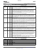
Figure 20. AC Link Output Frame
AC LINK OUTPUT FRAME:
SDATA_OUT, CONTROLLER OUTPUT TO LM4550 INPUT
The AC Link Output Frame carries control and PCM data to the LM4550 control registers and stereo DAC.
Output Frames are carried on the SDATA_OUT signal which is an output from the AC '97 Digital Controller and
an input to the LM4550 codec. As shown in Figure 19, Output Frames are constructed from thirteen time slots:
one Tag Slot followed by twelve Data Slots. Each Frame consists of 256 bits with each of the twelve Data Slots
containing 20 bits. Input and Output Frames are aligned to the same SYNC transition. Note that the LM4550 only
accepts data in eight of the twelve Data Slots and, since it is a two channel codec only in 4 simultaneously – 2
for control, one each for PCM data to the left and right channel DACs. Data-Slot to DAC mappings are tied to the
codec mode selected by the Identity pins ID1#, ID0# and are given in Table 19.
A new Output Frame is signaled with a low-to-high transition of SYNC. SYNC should be clocked from the
controller on a rising edge of BIT_CLK and, as shown in Figure 20 and Figure 21, the first tag bit in the Frame
(“Valid Frame”) should be clocked from the controller by the next rising edge of BIT_CLK and sampled by the
LM4550 on the following falling edge. The AC '97 Controller should always clock data to SDATA_OUT on a rising
edge of BIT_CLK and the LM4550 always samples SDATA_OUT on the next falling edge. SYNC is sampled with
the rising edge of BIT_CLK.
The LM4550 checks each Frame to ensure 256 bits are received. If a new Frame is detected (a low-to-high
transition on SYNC) before 256 bits are received from the old Frame then the new Frame is ignored i.e. the data
on SDATA_OUT is discarded until a valid new Frame is detected.
The LM4550 expects to receive data MSB first, in an MSB justified format.
SDATA_OUT: Slot 0 – Tag Phase
The first bit of Slot 0 is designated the "Valid Frame" bit. If this bit is 1, it indicates that the current Output Frame
contains at least one slot of valid data and the LM4550 will check further tag bits for valid data in the expected
Data Slots. With the codec in Primary mode, a controller will indicate valid data in a slot by setting the associated
tag bit equal to 1. Since it is a two channel codec the LM4550 can only receive data from four slots in a given
frame and so only checks the valid-data bits for 4 slots. In Primary mode these tag bits are for: slot 1 (Command
Address), slot 2 (Command Data), slot 3 (PCM data for left DAC) and slot 4 (PCM data for right DAC).
The last two bits in the Tag contain the Codec ID used to select the target codec to receive the frame in multiple
codec systems. When the frame is being sent to a codec in one of the Secondary modes the controller does not
use bits 14 and 13 to indicate valid Command Address and Data in slots 1 and 2. Instead, this role is performed
by the Codec ID bits – operation of the Extended AC Link assumes that the controller would not access a
secondary codec unless it was providing valid Command Address and/or Data. When in one of the secondary
modes the LM4550 only checks the tag bits for the Codec ID and for valid data in the two audio data slots: slots
3 & 4 for Secondary mode 1, slots 7 & 8 for mode 2 and slots 6 & 9 for mode 3.
When sending an Output Frame to a Secondary mode codec, a controller should set tag bits 14 and 13 to zero.
20 Submit Documentation Feedback Copyright © 2001–2013, Texas Instruments Incorporated
Product Folder Links: LM4550