
Datasheet


LM4132
www.ti.com
SNVS372C –AUGUST 2005–REVISED APRIL 2013
APPLICATION INFORMATION
THEORY OF OPERATION
The foundation of any voltage reference is the band-gap circuit. While the reference in the LM4132 is developed
from the gate-source voltage of transistors in the IC, principles of the band-gap circuit are easily understood
using a bipolar example. For a detailed analysis of the bipolar band-gap circuit, please refer to Application Note
AN-56.
SUPPLY AND ENABLE VOLTAGES
To ensure proper operation, V
EN
and V
IN
must be within a specified range. An acceptable range of input voltages
is:
V
IN
> V
REF
+ 400mV (I
LOAD
≤ 10mA) (1)
The enable pin uses an internal pull-up current source (I
PULL_UP
≊ 2µA) that may be left floating or triggered by an
external source. If the part is not enabled by an external source, it may be connected to V
IN
. An acceptable range
of enable voltages is given by the enable transfer characteristics. See the Electrical Characteristics section and
Enable Transfer Characteristics figure for more detail. Note, the part will not operate correctly for V
EN
> V
IN
.
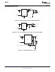
COMPONENT SELECTION
A small ceramic (X5R or X7R) capacitor on the input must be used to ensure stable operation. The value of C
IN
must be sized according to the output capacitor value. The value of C
IN
must satisfy the relationship C
IN
≥ C
OUT
.
When no output capacitor is used, C
IN
must have a minimum value of 0.1µF. Noise on the power-supply input
may affect the output noise. Larger input capacitor values (typically 4.7µF to 22µF) may help reduce noise on the
output and significantly reduce overshoot during startup. Use of an additional optional bypass capacitor between
the input and ground may help further reduce noise on the output. With an input capacitor, the LM4132 will drive
any combination of resistance and capacitance up to V
REF
/20mA and 10µF respectively.
The LM4132 is designed to operate with or without an output capacitor and is stable with capacitive loads up to
10µF. Connecting a capacitor between the output and ground will significantly improve the load transient
response when switching from a light load to a heavy load. The output capacitor should not be made arbitrarily
large because it will effect the turn-on time as well as line and load transients.
While a variety of capacitor chemistry types may be used, it is typically advisable to use low esr ceramic
capacitors. Such capacitors provide a low impedance to high frequency signals, effectively bypassing them to
ground. Bypass capacitors should be mounted close to the part. Mounting bypass capacitors close to the part will
help reduce the parasitic trace components thereby improving performance.
SHORT CIRCUITED OUTPUT
The LM4132 features indefinite short circuit protection. This protection limits the output current to 75mA when the
output is shorted to ground.
TURN ON TIME
Turn on time is defined as the time taken for the output voltage to rise to 90% of the preset value. The turn on
time depends on the load. The turn on time is typically 33.2µs when driving a 1µF load and 78.8µs when driving
a 10µF load. Some users may experience an extended turn on time (up to 10ms) under brown out conditions
and low temperatures (-40°C).
THERMAL HYSTERESIS
Thermal hysteresis is defined as the change in output voltage at 25ºC after some deviation from 25ºC. This is to
say that thermal hysteresis is the difference in output voltage between two points in a given temperature profile.
An illustrative temperature profile is shown in Figure 47.
Copyright © 2005–2013, Texas Instruments Incorporated Submit Documentation Feedback 17
Product Folder Links: LM4132