
Datasheet


LM4050-N, LM4050-N-Q1
www.ti.com
SNOS455E –MAY 2000–REVISED APRIL 2013
APPLICATIONS INFORMATION
The LM4050-N is a precision micro-power curvature-corrected bandgap shunt voltage reference. For space
critical applications, the LM4050-N is available in the sub-miniature SOT-23 surface-mount package. The
LM4050-N has been designed for stable operation without the need of an external capacitor connected between
the “+” pin and the “−” pin. If, however, a bypass capacitor is used, the LM4050-N remains stable. Reducing
design effort is the availability of several fixed reverse breakdown voltages: 2.048V, 2.500V, 4.096V, 5.000V,
8.192V, and 10.000V. The minimum operating current increases from 60 μA for the LM4050-N-2.0 to 100 μA for
the LM4050-N-10.0. All versions have a maximum operating current of 15 mA.
LM4050-Ns in the SOT-23 packages have a parasitic Schottky diode between pin 2 (−) and pin 3 (Die attach
interface contact). Therefore, pin 3 of the SOT-23 package must be left floating or connected to pin 2.
The 4.096V version allows single +5V 12-bit ADCs or DACs to operate with an LSB equal to 1 mV. For 12-bit
ADCs or DACs that operate on supplies of 10V or greater, the 8.192V version gives 2 mV per LSB.
The typical thermal hysteresis specification is defined as the change in +25°C voltage measured after thermal
cycling. The device is thermal cycled to temperature -40°C and then measured at 25°C. Next the device is
thermal cycled to temperature +125°C and again measured at 25°C. The resulting V
OUT
delta shift between the
25°C measurements is thermal hysteresis. Thermal hysteresis is common in precision references and is induced
by thermal-mechanical package stress. Changes in environmental storage temperature, operating temperature
and board mounting temperature are all factors that can contribute to thermal hysteresis.
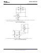
In a conventional shunt regulator application (Figure 12) , an external series resistor (R
S
) is connected between
the supply voltage and the LM4050-N. R
S
determines the current that flows through the load (I
L
) and the
LM4050-N (I
Q
). Since load current and supply voltage may vary, R
S
should be small enough to supply at least
the maximum guaranteed I
RMIN
(spec. table) to the LM4050-N even when the supply voltage is at its minimum
and the load current is at its maximum value. When the supply voltage is at its maximum and I
L
is at its
minimum, R
S
should be large enough so that the current flowing through the LM4050-N is less than 15 mA.
R
S
is determined by the supply voltage, (V
S
), the load and operating current, (I
L
and I
Q
), and the LM4050-N's
reverse breakdown voltage, V
R
.
(1)
Typical Applications
Figure 12. Shunt Regulator
Copyright © 2000–2013, Texas Instruments Incorporated Submit Documentation Feedback 11
Product Folder Links: LM4050-N LM4050-N-Q1