
Datasheet


I
CIN(RMS)
=
'i
L
/
3
(V
OUT
- V
IN
)V
IN
=
V
OUT
Lf
S
12
R
Gate
t
LH
=
V
DR
- Vgs
th
Qgs
2
Qgd +
x
P
SW
=
I
Lmax
x V
out
2
x f
SW
x (t
LH
+ t
HL
)
V
IN(MIN)
V
OUT
1-
D
MAX
=
I
OUT(max)
2
D
MAX
R
DS(ON)
P
COND(MAX)
=
1 - D
MAX
LM3481
SNVS346E –NOVEMBER 2007–REVISED APRIL 2012
www.ti.com
Power MOSFET Selection
The drive pin, DR, of the LM3481 must be connected to the gate of an external MOSFET. In a boost topology,
the drain of the external N-Channel MOSFET is connected to the inductor and the source is connected to the
ground. The drive pin voltage, V
DR
, depends on the input voltage (see typical performance characteristics). In
most applications, a logic level MOSFET can be used. For very low input voltages, a sub-logic level MOSFET
should be used.
The selected MOSFET directly controls the efficiency. The critical parameters for selection of a MOSFET are:
1. Minimum threshold voltage, V
TH(MIN)
2. On-resistance, R
DS(ON)
3. Total gate charge, Q
g
4. Reverse transfer capacitance, C
RSS
5. Maximum drain to source voltage, V
DS(MAX)
The off-state voltage of the MOSFET is approximately equal to the output voltage. V
DS(MAX)
of the MOSFET must
be greater than the output voltage. The power losses in the MOSFET can be categorized into conduction losses
and ac switching or transition losses. R
DS(ON)
is needed to estimate the conduction losses. The conduction loss,
P
COND
, is the I
2
R loss across the MOSFET. The maximum conduction loss is given by:
where D
MAX
is the maximum duty cycle.
At high switching frequencies the switching losses may be the largest portion of the total losses.
The switching losses are very difficult to calculate due to changing parasitics of a given MOSFET in operation.
Often, the individual MOSFET datasheet does not give enough information to yield a useful result. The following
formulas give a rough idea how the switching losses are calculated:
Input Capacitor Selection
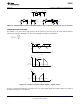
Due to the presence of an inductor at the input of a boost converter, the input current waveform is continuous
and triangular, as shown in Figure 30. The inductor ensures that the input capacitor sees fairly low ripple
currents. However, as the input capacitor gets smaller, the input ripple goes up. The rms current in the input
capacitor is given by:
The input capacitor should be capable of handling the rms current. Although the input capacitor is not as critical
in a boost application, low values can cause impedance interactions. Therefore a good quality capacitor should
be chosen in the range of 100 µF to 200 µF. If a value lower than 100 µF is used, then problems with impedance
interactions or switching noise can affect the LM3481. To improve performance, especially with V
IN
below 8V, it
is recommended to use a 20Ω resistor at the input to provide a RC filter. This resistor is placed in series with the
V
IN
pin with only a bypass capacitor attached to the V
IN
pin directly (see Figure 32). A 0.1 µF or 1 µF ceramic
capacitor is necessary in this configuration. The bulk input capacitor and inductor will connect on the other side
of the resistor with the input power supply.
18 Submit Documentation Feedback Copyright © 2007–2012, Texas Instruments Incorporated
Product Folder Links: LM3481