
Datasheet


LM117, LM317A, LM317-N
SNVS774O –MAY 2004–REVISED JANUARY 2014
www.ti.com
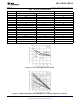
As a design aid, Figure 29 shows the maximum allowable power dissipation compared to ambient temperature
for the TO-263 device (assuming θ
(J−A)
is 35°C/W and the maximum junction temperature is 125°C).
Figure 29. Maximum Power Dissipation vs T
AMB
for the TO-263 Package
Heatsinking the TO-252 (NDP) Package
If the maximum allowable value for θ
JA
is found to be ≥103°C/W (Typical Rated Value) for the TO-252 package,
no heatsink is needed since the package alone will dissipate enough heat to satisfy these requirements. If the
calculated value for θ
JA
falls below these limits, a heatsink is required.
As a design aid, Table 1 shows the value of the θ
JA
of NDP the package for different heatsink area. The copper
patterns that we used to measure these θ
JA
s are shown in Figure 34. Figure 30 reflects the same test results as
what are in Table 1.
Figure 31 shows the maximum allowable power dissipation vs. ambient temperature for the TO-252 device.
Figure 32 shows the maximum allowable power dissipation vs. copper area (in
2
) for the TO-252 device. Please
see AN-1028 (literature number SNVA036) for thermal enhancement techniques to be used with SOT-223 and
TO-252 packages.
14 Submit Documentation Feedback Copyright © 2004–2014, Texas Instruments Incorporated
Product Folder Links: LM117 LM317A LM317-N