
Datasheet


LM2940-N, LM2940C
SNVS769I –MARCH 2000–REVISED APRIL 2013
www.ti.com
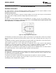
Figure 37. θ
(JA)
vs. Copper (1 ounce) Area for the DDPAK/TO-263 Package
As shown in the figure, increasing the copper area beyond 1 square inch produces very little improvement. It
should also be observed that the minimum value of θ
(JA)
for the DDPAK/TO-263 package mounted to a PCB is
32°C/W.
As a design aid, Figure 38 shows the maximum allowable power dissipation compared to ambient temperature
for the DDPAK/TO-263 device. This assumes a θ
(JA)
of 35°C/W for 1 square inch of 1 ounce copper and a
maximum junction temperature (T
J
) of 125°C.
Figure 38. Maximum Power Dissipation vs. T
A
for the DDPAK/TO-263 Package
HEATSINKING SOT-223 PACKAGE PARTS
The SOT-223 (DCY) packages use a copper plane on the PCB and the PCB itself as a heatsink. To optimize the
heat sinking ability of the plane and PCB, solder the tab of the package to the plane.
Figure 39 and Figure 40 show the information for the SOT-223 package. Figure 40 assumes a θ
(JA)
of 74°C/W
for 1 square inch of 1 ounce copper and 51°C/W for 1 square inch of 2 ounce copper, with a maximum ambient
temperature (T
A
) of 85°C and a maximum junction temperature (T
J
) of 125°C.
For techniques for improving the thermal resistance and power dissipation for the SOT-223 package, please
refer to Application Note AN-1028 (SNVA036).
16 Submit Documentation Feedback Copyright © 2000–2013, Texas Instruments Incorporated
Product Folder Links: LM2940-N LM2940C