
Datasheet


LM2738
BOOST
SW
GND
L
D1
D2
C
OUT
C
BOOST
V
OUT
C
IN
V
IN
V
IN
V
BOOST
LM2738
www.ti.com
SNVS556B –APRIL 2008–REVISED APRIL 2013
BOOST FUNCTION
Capacitor C
BOOST
and diode D2 in Figure 29 are used to generate a voltage V
BOOST
. V
BOOST
- V
SW
is the gate
drive voltage to the internal NMOS control switch. To properly drive the internal NMOS switch during its on-time,
V
BOOST
needs to be at least 2.5V greater than V
SW
. It is recommended that V
BOOST
be greater than 2.5V above
V
SW
for best efficiency. V
BOOST
– V
SW
should not exceed the maximum operating limit of 5.5V.
5.5V > V
BOOST
– V
SW
> 2.5V for best performance.
When the LM2738 starts up, internal circuitry from the BOOST pin supplies a maximum of 20mA to C
BOOST
. This
current charges C
BOOST
to a voltage sufficient to turn the switch on. The BOOST pin will continue to source
current to C
BOOST
until the voltage at the feedback pin is greater than 0.76V.
There are various methods to derive V
BOOST
:
1. From the input voltage (3.0V < V
IN
< 5.5V)
2. From the output voltage (2.5V < V
OUT
< 5.5V)
3. From an external distributed voltage rail (2.5V < V
EXT
< 5.5V)
4. From a shunt or series zener diode
In the Simplifed Block Diagram of (Figure 27), capacitor C
BOOST
and diode D2 supply the gate-drive voltage for
the NMOS switch. Capacitor C
BOOST
is charged via diode D2 by V
IN
. During a normal switching cycle, when the
internal NMOS control switch is off (T
OFF
) (refer to Figure 28), V
BOOST
equals V
IN
minus the forward voltage of D2
(V
FD2
), during which the current in the inductor (L) forward biases the Schottky diode D1 (V
FD1
). Therefore the
voltage stored across C
BOOST
is
V
BOOST
- V
SW
= V
IN
- V
FD2
+ V
FD1
(1)
When the NMOS switch turns on (T
ON
), the switch pin rises to
V
SW
= V
IN
– (R
DSON
x I
L
), (2)
forcing V
BOOST
to rise, thus reverse biasing D2. The voltage at V
BOOST
is then
V
BOOST
= 2V
IN
– (R
DSON
x I
L
) – V
FD2
+ V
FD1
(3)
which is approximately
2V
IN
- 0.4V (4)
for many applications. Thus the gate-drive voltage of the NMOS switch is approximately
V
IN
- 0.2V (5)
An alternate method for charging C
BOOST
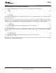
is to connect D2 to the output as shown in Figure 29. The output
voltage should be between 2.5V and 5.5V, so that proper gate voltage will be applied to the internal switch. In
this circuit, C
BOOST
provides a gate drive voltage that is slightly less than V
OUT
.
Figure 29. V
OUT
Charges C
BOOST
In applications where both V
IN
and V
OUT
are greater than 5.5V, or less than 3V, C
BOOST
cannot be charged
directly from these voltages. If V
IN
and V
OUT
are greater than 5.5V, C
BOOST
can be charged from V
IN
or V
OUT
minus a zener voltage by placing a zener diode D3 in series with D2, as shown in Figure 30. When using a
series zener diode from the input, ensure that the regulation of the input supply doesn’t create a voltage that falls
outside the recommended V
BOOST
voltage.
(V
INMAX
– V
D3
) < 5.5V
(V
INMIN
– V
D3
) > 2.5V
Copyright © 2008–2013, Texas Instruments Incorporated Submit Documentation Feedback 11
Product Folder Links: LM2738