
Datasheet
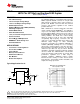


V
IN
BOOST
SW
GND
C
BOOST
L
D1
D2
D3
V
BOOST
V
IN
C
IN
C
OUT
V
OUT
LM2736
www.ti.com
SNVS316F –SEPTEMBER 2004–REVISED APRIL 2013
When the NMOS switch turns on (T
ON
), the switch pin rises to
V
SW
= V
IN
– (R
DSON
x I
L
), (2)
forcing V
BOOST
to rise thus reverse biasing D2. The voltage at V
BOOST
is then
V
BOOST
= 2V
IN
– (R
DSON
x I
L
) – V
FD2
+ V
FD1
(3)
which is approximately
2V
IN
- 0.4V (4)
for many applications. Thus the gate-drive voltage of the NMOS switch is approximately
V
IN
- 0.2V (5)
An alternate method for charging C
BOOST
is to connect D2 to the output as shown in Figure 21. The output
voltage should be between 2.5V and 5.5V, so that proper gate voltage will be applied to the internal switch. In
this circuit, C
BOOST
provides a gate drive voltage that is slightly less than V
OUT
.
In applications where both V
IN
and V
OUT
are greater than 5.5V, or less than 3V, C
BOOST
cannot be charged
directly from these voltages. If V
IN
and V
OUT
are greater than 5.5V, C
BOOST
can be charged from V
IN
or V
OUT
minus a zener voltage by placing a zener diode D3 in series with D2, as shown in Figure 22. When using a
series zener diode from the input, ensure that the regulation of the input supply doesn’t create a voltage that falls
outside the recommended V
BOOST
voltage.
(V
INMAX
– V
D3
) < 5.5V
(V
INMIN
– V
D3
) > 1.6V
Figure 22. Zener Reduces Boost Voltage from V
IN
An alternative method is to place the zener diode D3 in a shunt configuration as shown in Figure 23. A small
350mW to 500mW 5.1V zener in a SOT or SOD package can be used for this purpose. A small ceramic
capacitor such as a 6.3V, 0.1µF capacitor (C4) should be placed in parallel with the zener diode. When the
internal NMOS switch turns on, a pulse of current is drawn to charge the internal NMOS gate capacitance. The
0.1 µF parallel shunt capacitor ensures that the V
BOOST
voltage is maintained during this time.
Resistor R3 should be chosen to provide enough RMS current to the zener diode (D3) and to the BOOST pin. A
recommended choice for the zener current (I
ZENER
) is 1 mA. The current I
BOOST
into the BOOST pin supplies the
gate current of the NMOS control switch and varies typically according to the following formula for the X -
version:
I
BOOST
= 0.49 x (D + 0.54) x (V
ZENER
– V
D2
) mA (6)
I
BOOST
can be calculated for the Y version using the following:
I
BOOST
= 0.20 x (D + 0.54) x (V
ZENER
- V
D2
) µA (7)
where D is the duty cycle, V
ZENER
and V
D2
are in volts, and I
BOOST
is in milliamps. V
ZENER
is the voltage applied to
the anode of the boost diode (D2), and V
D2
is the average forward voltage across D2. Note that this formula for
I
BOOST
gives typical current. For the worst case I
BOOST
, increase the current by 40%. In that case, the worst case
boost current will be
I
BOOST-MAX
= 1.4 x I
BOOST
(8)
R3 will then be given by
R3 = (V
IN
- V
ZENER
) / (1.4 x I
BOOST
+ I
ZENER
) (9)
For example, using the X-version let V
IN
= 10V, V
ZENER
= 5V, V
D2
= 0.7V, I
ZENER
= 1mA, and duty cycle D = 50%.
Then
Copyright © 2004–2013, Texas Instruments Incorporated Submit Documentation Feedback 9
Product Folder Links: LM2736