
Datasheet

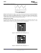


Table Of Contents
- FEATURES
- Applications
- DESCRIPTION
- Absolute Maximum Ratings
- Electrical Characteristics
- Typical Performance Characteristics
- Block Diagram
- Theory of Operation
- Application Hints
- SELECTING THE EXTERNAL CAPACITORS
- SELECTING THE OUTPUT CAPACITOR
- SELECTING THE INPUT CAPACITOR
- FEED-FORWARD COMPENSATION
- SELECTING DIODES
- LAYOUT HINTS
- SETTING THE OUTPUT VOLTAGE
- SWITCHING FREQUENCY
- DUTY CYCLE
- INDUCTANCE VALUE
- MAXIMUM SWITCH CURRENT
- CALCULATING LOAD CURRENT
- DESIGN PARAMETERS VSW AND ISW
- THERMAL CONSIDERATIONS
- MINIMUM INDUCTANCE
- INDUCTOR SUPPLIERS
- SHUTDOWN PIN OPERATION
- Application Hints
- Revision History

Duty Cycle =
V
OUT
+ V
DIODE
- V
IN
V
OUT
+ V
DIODE
- V
SW
LM2733
www.ti.com
SNVS209E –NOVEMBER 2002–REVISED APRIL 2013
DUTY CYCLE
The maximum duty cycle of the switching regulator determines the maximum boost ratio of output-to-input
voltage that the converter can attain in continuous mode of operation. The duty cycle for a given boost
application is defined as:
(3)
This applies for continuous mode operation.
The equation shown for calculating duty cycle incorporates terms for the FET switch voltage and diode forward
voltage. The actual duty cycle measured in operation will also be affected slightly by other power losses in the
circuit such as wire losses in the inductor, switching losses, and capacitor ripple current losses from self-heating.
Therefore, the actual (effective) duty cycle measured may be slightly higher than calculated to compensate for
these power losses. A good approximation for effctive duty cycle is :
DC (eff) = (1 - Efficiency x (V
IN
/V
OUT
)) (4)
Where the efficiency can be approximated from the curves provided.
INDUCTANCE VALUE
The first question we are usually asked is: “How small can I make the inductor?” (because they are the largest
sized component and usually the most costly). The answer is not simple and involves tradeoffs in performance.
Larger inductors mean less inductor ripple current, which typically means less output voltage ripple (for a given
size of output capacitor). Larger inductors also mean more load power can be delivered because the energy
stored during each switching cycle is:
E =L/2 X (lp)
2
(5)
Where “lp” is the peak inductor current. An important point to observe is that the LM2733 will limit its switch
current based on peak current. This means that since lp(max) is fixed, increasing L will increase the maximum
amount of power available to the load. Conversely, using too little inductance may limit the amount of load
current which can be drawn from the output.
Best performance is usually obtained when the converter is operated in “continuous” mode at the load current
range of interest, typically giving better load regulation and less output ripple. Continuous operation is defined as
not allowing the inductor current to drop to zero during the cycle. It should be noted that all boost converters shift
over to discontinuous operation as the output load is reduced far enough, but a larger inductor stays “continuous”
over a wider load current range.
To better understand these tradeoffs, a typical application circuit (5V to 12V boost with a 10 µH inductor) will be
analyzed. We will assume:
V
IN
= 5V, V
OUT
= 12V, V
DIODE
= 0.5V, V
SW
= 0.5V
Since the frequency is 1.6 MHz (nominal), the period is approximately 0.625 µs. The duty cycle will be 62.5%,
which means the ON time of the switch is 0.390 µs. It should be noted that when the switch is ON, the voltage
across the inductor is approximately 4.5V.
Using the equation:
V = L (di/dt) (6)
We can then calculate the di/dt rate of the inductor which is found to be 0.45 A/µs during the ON time. Using
these facts, we can then show what the inductor current will look like during operation:
Copyright © 2002–2013, Texas Instruments Incorporated Submit Documentation Feedback 11
Product Folder Links: LM2733