
Datasheet


SW
BST
NC
NC
NC
NC
RTN
FB
SS
11
10
9
5
4
3
2
1
6
7 8
12
13
14
VCC
VIN
RON/SD
SGND
ISEN
SW
BST
RTN
VCC
FB
SS
VIN
10
9
8
7
6
5
4
3
2
1
RON/SD
SGND
ISEN
LM2695
SNVS413A –JANUARY 2006–REVISED APRIL 2013
www.ti.com
Connection Diagram
Figure 1. 14-Lead HTSSOP (Top View) Figure 2. 10-Lead WSON (Top View)
See PWP0014A Package See DPR0010A Package
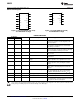
PIN DESCRIPTIONS
Pin Number
Name Description Application Information
WSON-10 HTSSOP-14
1 2 SW Switching Node Internally connected to the buck switch source.
Connect to the inductor, free-wheeling diode, and
bootstrap capacitor.
2 3 BST Boost pin for bootstrap capacitor Connect a 0.022 µF capacitor from SW to this pin.
The capacitor is charged from V
CC
via an internal
diode during each off-time.
3 4 I
SEN
Current sense The re-circulating current flows through the internal
sense resistor, and out of this pin to the free-wheeling
diode. Current limit is nominally set at 1.25A.
4 5 S
GND
Sense Ground Re-circulating current flows into this pin to the current
sense resistor.
5 6 RTN Circuit Ground Ground for all internal circuitry other than the current
limit detection.
6 9 FB Feedback input from the regulated Internally connected to the regulation and over-
output voltage comparators. The regulation level is 2.5V.
7 10 SS Softstart An internal 12.3 µA current source charges an
external capacitor to 2.5V, providing the softstart
function.
8 11 R
ON
/SD On-time control and shutdown An external resistor from V
IN
to this pin sets the buck
switch on-time. Grounding this pin shuts down the
regulator.
9 12 V
CC
Output from the startup regulator Nominally regulates at 7.0V. An external voltage (8V-
14V) can be applied to this pin to reduce internal
dissipation. An internal diode connects V
CC
to V
IN
.
10 13 V
IN
Input supply voltage Nominal input range is 8.0V to 30V.
1,7,8,14 NC No connection. No internal connection.
EP Exposed Pad Exposed metal pad on the underside of the device. It
is recommended to connect this pad to the PC board
ground plane to aid in heat dissipation.
These devices have limited built-in ESD protection. The leads should be shorted together or the device placed in conductive foam
during storage or handling to prevent electrostatic damage to the MOS gates.
2 Submit Documentation Feedback Copyright © 2006–2013, Texas Instruments Incorporated
Product Folder Links: LM2695