
Datasheet


-60
-40
-20
0
20
0.01 0.1 1 10 100
FREQUENCY (kHz)
GAIN (dB)
1000
0
-45
-90
-135
-180
PHASE (º)
fp
fz
fn
LM26001, LM26001Q
www.ti.com
SNVS430G –MAY 2006–REVISED MAY 2006
BOOTSTRAP
The drive voltage for the internal switch is supplied via the BOOT pin. This pin must be connected to a ceramic
capacitor, Cboot, from the switch node, shown as C4 in the typical application. The LM26001 provides the VDD
voltage internally, so no external diode is needed. A maximum value of 0.1 uF is recommended for Cboot.
Values smaller than 0.01 uF may result in insufficient hold up time for the drive voltage and increased power
dissipation.
During low Vin operation, when the on-time is extended, the bootstrap capacitor is at risk of discharging. If the
Cboot capacitor is discharged below approximately 2.5V, the LM26001 enters a high frequency re-charge mode.
The Cboot cap is re-charged via the LG synchronous FET shown in the block diagram. Switching returns to
normal when the Cboot cap has been recharged.
CATCH DIODE
When the internal switch is off, output current flows through the catch diode. Alternately, when the switch is on,
the diode sees a reverse voltage equal to Vin. Therefore, the important parameters for selecting the catch diode
are peak current and peak inverse voltage. The average current through the diode is given by:
ID
AVE
= Iload x (1-D) (16)
Where D is the duty cycle, defined as Vout/Vin. The catch diode conducts the largest currents during the lowest
duty cycle. Therefore ID
AVE
should be calculated assuming maximum input voltage. The diode should be rated to
handle this current continuously. For over-current or short circuit conditions, the catch diode should be rated to
handle peak currents equal to the peak current limit.
The peak inverse voltage rating of the diode must be greater than maximum input voltage.
A Schottky diode must be used. It's low forward voltage maximizes efficiency and BOOT voltage, while also
protecting the SW pin against large negative voltage spikes.
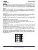
COMPENSATION
The purpose of loop compensation is to ensure stable operation while maximizing dynamic performance. Stability
can be analyzed with loop gain measurements, while dynamic performance is analyzed with both loop gain and
load transient response. Loop gain is equal to the product of control-output transfer function (power stage) and
the feedback transfer function (the compensation network).
For stability purposes, our target is to have a loop gain slope that is -20dB /decade from a very low frequency to
beyond the crossover frequency. Also, the crossover frequency should not exceed one-fifth of the switching
frequency, i.e. 60 kHz in the case of 300 kHz switching frequency.
For dynamic purposes, the higher the bandwidth, the faster the load transient response. A large DC gain means
high DC regulation accuracy (i.e. DC voltage changes little with load or line variations). To achieve this loop gain,
the compensation components should be set according to the shape of the control-output bode plot. A typical
plot is shown in Figure 22.
Figure 22. Control-Output Transfer Function
Copyright © 2006, Texas Instruments Incorporated Submit Documentation Feedback 17
Product Folder Links: LM26001 LM26001Q