
Datasheet


LM2599
www.ti.com
SNVS123C –APRIL 1998–REVISED APRIL 2013
Discontinuous operation can have voltage waveforms that are considerable different than a continuous design.
The output pin (switch) waveform can have some damped sinusoidal ringing present. (See Typical Performance
Characteristics photo titled Discontinuous Mode Switching Waveforms) This ringing is normal for discontinuous
operation, and is not caused by feedback loop instabilities. In discontinuous operation, there is a period of time
where neither the switch or the diode are conducting, and the inductor current has dropped to zero. During this
time, a small amount of energy can circulate between the inductor and the switch/diode parasitic capacitance
causing this characteristic ringing. Normally this ringing is not a problem, unless the amplitude becomes great
enough to exceed the input voltage, and even then, there is very little energy present to cause damage.
Different inductor types and/or core materials produce different amounts of this characteristic ringing. Ferrite core
inductors have very little core loss and therefore produce the most ringing. The higher core loss of powdered iron
inductors produce less ringing. If desired, a series RC could be placed in parallel with the inductor to dampen the
ringing. The computer aided design software Switchers Made Simple (version 4.3) will provide all component
values for continuous and discontinuous modes of operation.
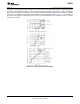
Figure 36. Post Ripple Filter Waveform
OUTPUT VOLTAGE RIPPLE AND TRANSIENTS
The output voltage of a switching power supply operating in the continuous mode will contain a sawtooth ripple
voltage at the switcher frequency, and may also contain short voltage spikes at the peaks of the sawtooth
waveform.
The output ripple voltage is a function of the inductor sawtooth ripple current and the ESR of the output
capacitor. A typical output ripple voltage can range from approximately 0.5% to 3% of the output voltage. To
obtain low ripple voltage, the ESR of the output capacitor must be low, however, caution must be exercised when
using extremely low ESR capacitors because they can affect the loop stability, resulting in oscillation problems. If
very low output ripple voltage is needed (less than 20 mV), a post ripple filter is recommended (See Figure 24).
The inductance required is typically between 1 μH and 5 μH, with low DC resistance, to maintain good load
regulation. A low ESR output filter capacitor is also required to assure good dynamic load response and ripple
reduction. The ESR of this capacitor may be as low as desired, because it is out of the regulator feedback loop.
The photo shown in Figure 36 shows a typical output ripple voltage, with and without a post ripple filter.
When observing output ripple with a scope, it is essential that a short, low inductance scope probe ground
connection be used. Most scope probe manufacturers provide a special probe terminator which is soldered onto
the regulator board, preferable at the output capacitor. This provides a very short scope ground thus eliminating
the problems associated with the 3 inch ground lead normally provided with the probe, and provides a much
cleaner and more accurate picture of the ripple voltage waveform.
The voltage spikes are caused by the fast switching action of the output switch, the diode, and the parasitic
inductance of the output filter capacitor, and its associated wiring. To minimize these voltage spikes, the output
capacitor should be designed for switching regulator applications, and the lead lengths must be kept very short.
Wiring inductance, stray capacitance, as well as the scope probe used to evaluate these transients, all contribute
to the amplitude of these spikes.
Copyright © 1998–2013, Texas Instruments Incorporated Submit Documentation Feedback 27
Product Folder Links: LM2599