
Datasheet


LM2594, LM2594HV
www.ti.com
SNVS118C –DECEMBER 1999–REVISED APRIL 2013
The curves shown in Figure 31 and Figure 32 show the LM2594 junction temperature rise above ambient
temperature with a 500 mA load for various input and output voltages. This data was taken with the circuit
operating as a buck switcher with all components mounted on a PC board to simulate the junction temperature
under actual operating conditions. This curve is typical, and can be used for a quick check on the maximum
junction temperature for various conditions, but keep in mind that there are many factors that can affect the
junction temperature.
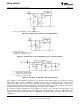
Figure 33. Delayed Startup
Figure 34. Undervoltage Lockout
for Buck Regulator
DELAYED STARTUP
The circuit in Figure 33 uses the the ON /OFF pin to provide a time delay between the time the input voltage is
applied and the time the output voltage comes up (only the circuitry pertaining to the delayed start up is shown).
As the input voltage rises, the charging of capacitor C1 pulls the ON /OFF pin high, keeping the regulator off.
Once the input voltage reaches its final value and the capacitor stops charging, and resistor R
2
pulls the ON
/OFF pin low, thus allowing the circuit to start switching. Resistor R
1
is included to limit the maximum voltage
applied to the ON /OFF pin (maximum of 25V), reduces power supply noise sensitivity, and also limits the
capacitor, C1, discharge current. When high input ripple voltage exists, avoid long delay time, because this ripple
can be coupled into the ON /OFF pin and cause problems.
This delayed startup feature is useful in situations where the input power source is limited in the amount of
current it can deliver. It allows the input voltage to rise to a higher voltage before the regulator starts operating.
Buck regulators require less input current at higher input voltages.
UNDERVOLTAGE LOCKOUT
Some applications require the regulator to remain off until the input voltage reaches a predetermined voltage. An
undervoltage lockout feature applied to a buck regulator is shown in Figure 34, while Figure 35 and Figure 36
applies the same feature to an inverting circuit. The circuit in Figure 35 features a constant threshold voltage for
turn on and turn off (zener voltage plus approximately one volt). If hysteresis is needed, the circuit in Figure 36
has a turn ON voltage which is different than the turn OFF voltage. The amount of hysteresis is approximately
equal to the value of the output voltage. If zener voltages greater than 25V are used, an additional 47 kΩ resistor
is needed from the ON /OFF pin to the ground pin to stay within the 25V maximum limit of the ON /OFF pin.
INVERTING REGULATOR
The circuit in Figure 37 converts a positive input voltage to a negative output voltage with a common ground. The
circuit operates by bootstrapping the regulators ground pin to the negative output voltage, then grounding the
feedback pin, the regulator senses the inverted output voltage and regulates it.
Copyright © 1999–2013, Texas Instruments Incorporated Submit Documentation Feedback 27
Product Folder Links: LM2594 LM2594HV