
Datasheet


( )
6
IN OUT IN OUT
PEAK LOAD
IN
IN OUT
V V V V 10
I I
V
2 L f V V
æ ö
+ ´ ´
= ´ +
ç ÷
´ ´ ´ +
è ø
LM2591HV
SNVS074D –MAY 2001–REVISED APRIL 2013
www.ti.com
(Adjustable Output Voltage Version)
lNVERTING REGULATOR
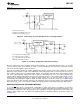
The circuit in Figure 33 converts a positive input voltage to a negative output voltage with a common ground. The
circuit operates by bootstrapping the regulator's ground pin to the negative output voltage, then grounding the
feedback pin, the regulator senses the inverted output voltage and regulates it.
This example uses the LM2591HV-5.0 to generate a −5V output, but other output voltages are possible by
selecting other output voltage versions, including the adjustable version. Since this regulator topology can
produce an output voltage that is either greater than or less than the input voltage, the maximum output current
greatly depends on both the input and output voltage.
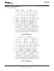
To determine how much load current is possible before the internal device current limit is reached (and power
limiting occurs), the system must be evaluated as a buck-boost configuration rather than as a buck. The peak
switch current in Amperes, for such a configuration is given as:
where
• L is in μH
• and f is in Hz
• The maximum possible load current I
LOAD
is limited by the requirement that I
PEAK
≤ I
CLIM
(8)
While checking for this, take I
CLIM
to be the lowest possible current limit value (min across tolerance and
temperature is 1.2A for the LM2591HV). Also to account for inductor tolerances, we should take the min value of
Inductance for L in Equation 8 (typically 20% less than the nominal value). Further, Equation 8 disregards the
drop across the Switch and the diode. This is equivalent to assuming 100% efficiency, which is never so.
Therefore expect I
PEAK
to be an additional 10-20% higher than calculated from Equation 8.
The reader is also referred to Application Note AN-1157 SNVA022 for examples based on positive to negative
configuration.
The maximum voltage appearing across the regulator is the absolute sum of the input and output voltage, and
this must be limited to a maximum of 60V. For example, when converting +20V to −12V, the regulator would see
32V between the input pin and ground pin. The LM2591HV has a maximum input voltage spec of 60V.
Additional diodes are required in this regulator configuration. Diode D1 is used to isolate input voltage ripple or
noise from coupling through the C
IN
capacitor to the output, under light or no load conditions. Also, this diode
isolation changes the topology to closley resemble a buck configuration thus providing good closed loop stability.
A Schottky diode is recommended for low input voltages, (because of its lower voltage drop) but for higher input
voltages, a fast recovery diode could be used.
Without diode D3, when the input voltage is first applied, the charging current of C
IN
can pull the output positive
by several volts for a short period of time. Adding D3 prevents the output from going positive by more than a
diode voltage.
18 Submit Documentation Feedback Copyright © 2001–2013, Texas Instruments Incorporated
Product Folder Links: LM2591HV