
Datasheet


I
PP
I
O
0
T =
1
f
SW
R
T
=
- 450 ns
284 pF
1
250 kHz
= 12.5 k:
LM25116
SNVS509D –APRIL 2007–REVISED FEBRUARY 2013
www.ti.com
In some applications it may be desirable to slow down the high-side MOSFET turn-on time in order to control
switching spikes. This may be accomplished by adding a resistor is series with the HO output to the high-side
gate. Values greater than 10Ω should be avoided so as not to interfere with the adaptive gate drive. Use of an
HB resistor for this function should be carefully evaluated so as not cause potentially harmful negative voltage to
the high-side driver, and is generally limited to 2.2Ω maximum.
Thermal Protection
Internal thermal shutdown circuitry is provided to protect the integrated circuit in the event the maximum junction
temperature is exceeded. When activated, typically at 170°C, the controller is forced into a low power reset state,
disabling the output driver and the bias regulator. This is designed to prevent catastrophic failures from
accidental device overheating.
APPLICATION INFORMATION
EXTERNAL COMPONENTS
The procedure for calculating the external components is illustrated with the following design example. The Bill of
Materials for this design is listed in Table 1. The circuit shown in Figure 41 is configured for the following
specifications:
• Output voltage = 5V
• Input voltage = 7V to 42V
• Maximum load current = 7A
• Switching frequency = 250 kHz
Simplified equations are used as a general guideline for the design method. Comprehensive equations are
provided in Comprehensive Equations.
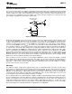
TIMING RESISTOR
R
T
sets the oscillator switching frequency. Generally, higher frequency applications are smaller but have higher
losses. Operation at 250 kHz was selected for this example as a reasonable compromise for both small size and
high efficiency. The value of R
T
for 250 kHz switching frequency can be calculated as follows:
(7)
The nearest standard value of 12.4 kΩ was chosen for R
T
.
OUTPUT INDUCTOR
The inductor value is determined based on the operating frequency, load current, ripple current and the input and
output voltages.
Figure 35. Inductor Current
18 Submit Documentation Feedback Copyright © 2007–2013, Texas Instruments Incorporated
Product Folder Links: LM25116