
Datasheet


LM25037, LM25037-Q1
www.ti.com
SNVS572D –JULY 2008–REVISED MARCH 2013
PIN DESCRIPTIONS (continued)
Pin Name Description Application Information
16 VIN Input voltage source Input to the VCC Start-up regulator. Operating input range is 5.5V to 75V. For
power sources outside of this range, the LM25037 can be biased directly at
VCC by an external regulator.
These devices have limited built-in ESD protection. The leads should be shorted together or the device placed in conductive foam
during storage or handling to prevent electrostatic damage to the MOS gates.
Absolute Maximum Ratings
(1)(2)
VIN to GND -0.3V to 76V
VCC, RAMP , OUTA, OUTB to GND -0.3V to 16V
CS to GND -0.3V to 1.0V
UVLO, FB, RT2, RT1, SS, REF to GND -0.3V to 7V
COMP, RES
(3)
ESD Rating
(4)
Human Body Model 2kV
Storage Temperature Range −65°C to + 150°C
Junction Temperature 150°C
(1) Absolute Maximum Ratings are limits beyond which damage to the device may occur. Operating Ratings are conditions under which
operation of the device is intended to be functional. For ensured specifications and test conditions, see the Electrical Characteristics.
(2) If Military/Aerospace specified devices are required, please contact the Texas Instruments Sales Office/ Distributors for availability and
specifications.
(3) COMP, RES are output pins. As such, it is not recommended that external power sources be connected to these pins.
(4) The human body model is a 100 pF capacitor discharged through a 1.5 kΩ resistor into each pin. 2kV for all pins.
Operating Ratings
VIN Voltage 5.5V to 75V
External Voltage Applied to VCC 8V to 14V
Operation Junction Temperature −40°C to + 125°C
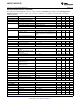
Electrical Characteristics
Specifications with standard typeface are for T
J
= 25°C, and those with boldface type apply over full operating junction
temperature range of −40°C to + 125°C. V
VIN
= 12V, V
VCC
= 10V, R
RT1
= 30.1 kΩ, R
RT2
= 30.1 kΩ, V
UVLO
= 3V unless
otherwise stated.
(1)(2)
Symbol Parameter Conditions Min Typ Max Units
Startup Regulator (VCC Pin)
V
VCC
VCC voltage I
VCC
= 10 mA 7.2 7.7 8.1 V
I
VCC(Lim)
VCC current limit V
VCC
= 7V 20 mA
V
VCC(UV)
VCC Under-voltage threshold 4.6 5 5.4 V
Hysteresis 0.5 V
I
VIN
Startup regulator current V
VIN
= 20V, V
UVLO
= 0V 35 58 µA
V
VIN
= 75V, V
UVLO
= 0V 45 80 µA
Supply current into VCC from Outputs & COMP open, V
VCC
= 10V, 4 mA
external source Outputs switching
Voltage Reference Regulator (REF Pin)
V
REF
REF Voltage I
REF
= 0 mA 4.75 5 5.15 V
REF Voltage Regulation I
REF
= 0 to 2.5 mA 7 25 mV
I
REF(Lim)
REF Current Limit V
REF
= 4.5V 5 10 mA
VREF Under-Voltage Threshold 3.7 4 4.3 V
(1) All limits are ensured. All electrical characteristics having room temperature limits are tested during production at T
A
= 25°C. All hot and
cold limits are ensured by correlating the electrical characteristics to process and temperature variations and applying statistical process
control.
(2) Typical specifications represent the most likely parametric norm at 25°C operation.
Copyright © 2008–2013, Texas Instruments Incorporated Submit Documentation Feedback 3
Product Folder Links: LM25037 LM25037-Q1