
Datasheet


REF LEVEL
0.000 dB
0.0 deg
100 1k
START 50.000 Hz
10k
STOP 50 000.000 Hz
/DIV
10.000 dB
45.000 deg
0
GAIN
PHASE
LM25005
www.ti.com
SNVS411C –JANUARY 2006–REVISED MARCH 2013
R4, C5, C6
These components configure the error amplifier gain characteristics to accomplish a stable overall loop gain. One
advantage of current mode control is the ability to close the loop with only two feedback components, R4 and C5.
The overall loop gain is the product of the modulator gain and the error amplifier gain. The DC modulator gain of
the LM25005 is as follows:
DC Gain
(MOD)
= G
m(MOD)
x R
LOAD
= 2 x R
LOAD
(11)
The dominant low frequency pole of the modulator is determined by the load resistance (R
LOAD
,) and output
capacitance (C
OUT
). The corner frequency of this pole is:
f
p(MOD)
= 1 / (2π R
LOAD
C
OUT
) (12)
For R
LOAD
= 5 Ω and C
OUT
= 177 µF then f
p(MOD)
= 180Hz
DC Gain
(MOD)
= 2 x 5 = 10 = 20 dB
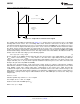
For the design example of Typical Application Circuit and Block Diagram the following modulator gain vs.
frequency characteristic was measured as shown in Figure 16.
Figure 16. Gain and Phase of Modulator
R
LOAD
= 5 Ohms and C
OUT
= 177 µF
Components R4 and C5 configure the error amplifier as a type II configuration which has a pole at DC and a
zero at f
Z
= 1 / (2πR4C5). The error amplifier zero cancels the modulator pole leaving a single pole response at
the crossover frequency of the loop gain. A single pole response at the crossover frequency yields a very stable
loop with 90 degrees of phase margin.
For the design example, a target loop bandwidth (crossover frequency) of 20 kHz was selected. The
compensation network zero (f
Z
) should be selected at least an order of magnitude less than the target crossover
frequency. This constrains the product of R4 and C5 for a desired compensation network zero 1 / (2π R4 C5) to
be less than 2kHz. Increasing R4 while proportionally decreasing C5, increases the error amp gain. Conversely,
decreasing R4 while proportionally increasing C5, decreases the error amp gain. For the design example C5 was
selected for 0.01µF and R4 was selected for 49.9 kΩ. These values configure the compensation network zero at
320 Hz. The error amp gain at frequencies greater than f
Z
is: R4 / R5, which is approximately 10 (20dB).
Copyright © 2006–2013, Texas Instruments Incorporated Submit Documentation Feedback 17
Product Folder Links: LM25005