
Datasheet


LOGIC
OSC
+
-
TYPE III
COMP
+
-
1.285V
&
Soft-start
INT REG, EN,UVLO
GND
SW
BOOT
VIN
EN
FB
VIN
VOUT
Error Amp.
PWM Cmp.
V
cc
ILimit
LM22675
www.ti.com
SNVS591K –SEPTEMBER 2008–REVISED MARCH 2013
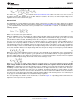
Simplified Block Diagram
Figure 11. Simplified Block Diagram
Detailed Operating Description
The LM22675 incorporates a voltage mode constant frequency PWM architecture. In addition, input voltage feed-
forward is used to stabilize the loop gain against variations in input voltage. This allows the loop compensation to
be optimized for transient performance. The power MOSFET, in conjunction with the diode, produce a
rectangular waveform at the switch pin, that swings from about zero volts to VIN. The inductor and output
capacitor average this waveform to become the regulator output voltage. By adjusting the duty cycle of this
waveform, the output voltage can be controlled. The error amplifier compares the output voltage with the internal
reference and adjusts the duty cycle to regulate the output at the desired value.
The internal loop compensation of the -ADJ option is optimized for outputs of 5V and below. If an output voltage
of 5V or greater is required, the -5.0 option can be used with an external voltage divider. The minimum output
voltage is equal to the reference voltage; 1.285V (typ.).
The functional block diagram of the LM22675 is shown in Figure 11 .
Precision Enable and UVLO
The precision enable input (EN) is used to control the regulator. The precision feature allows simple sequencing
of multiple power supplies with a resistor divider from another supply. Connecting this pin to ground or to a
voltage less than 1.6V (typ.) will turn off the regulator. The current drain from the input supply, in this state, is 25
µA (typ.) at an input voltage of 12V. The EN input has an internal pull-up of about 6 µA. Therefore this pin can be
left floating or pulled to a voltage greater than 2.2V (typ.) to turn the regulator on. The hysteresis on this input is
about 0.6V (typ.) above the 1.6V (typ.) threshold. When driving the enable input, the voltage must never exceed
the 6V absolute maximum specification for this pin.
Copyright © 2008–2013, Texas Instruments Incorporated Submit Documentation Feedback 7
Product Folder Links: LM22675