
Datasheet


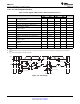


Table Of Contents
- 1 Device Overview
- Table of Contents
- 2 Revision History
- 3 Device Comparison
- 4 Terminal Configuration and Functions
- 4.1 PGE QFP Package Pinout (144-Pin)
- 4.2 ZWT BGA Package Ball-Map (337 Ball Grid Array)
- 4.3 Terminal Functions
- 4.3.1 PGE Package
- 4.3.1.1 Multibuffered Analog-to-Digital Converters (MibADC)
- 4.3.1.2 Enhanced High-End Timer Modules (N2HET)
- 4.3.1.3 Enhanced Capture Modules (eCAP)
- 4.3.1.4 Enhanced Quadrature Encoder Pulse Modules (eQEP)
- 4.3.1.5 Enhanced Pulse-Width Modulator Modules (ePWM)
- 4.3.1.6 General-Purpose Input / Output (GPIO)
- 4.3.1.7 Controller Area Network Controllers (DCAN)
- 4.3.1.8 Local Interconnect Network Interface Module (LIN)
- 4.3.1.9 Standard Serial Communication Interface (SCI)
- 4.3.1.10 Inter-Integrated Circuit Interface Module (I2C)
- 4.3.1.11 Standard Serial Peripheral Interface (SPI)
- 4.3.1.12 Multibuffered Serial Peripheral Interface Modules (MibSPI)
- 4.3.1.13 Ethernet Controller
- 4.3.1.14 USB Host and Device Port Controller Interface
- 4.3.1.15 System Module Interface
- 4.3.1.16 Clock Inputs and Outputs
- 4.3.1.17 Test and Debug Modules Interface
- 4.3.1.18 Flash Supply and Test Pads
- 4.3.1.19 Supply for Core Logic: 1.2V nominal
- 4.3.1.20 Supply for I/O Cells: 3.3V nominal
- 4.3.1.21 Ground Reference for All Supplies Except VCCAD
- 4.3.2 ZWT Package
- 4.3.2.1 Multibuffered Analog-to-Digital Converters (MibADC)
- 4.3.2.2 Enhanced High-End Timer Modules (N2HET)
- 4.3.2.3 Enhanced Capture Modules (eCAP)
- 4.3.2.4 Enhanced Quadrature Encoder Pulse Modules (eQEP)
- 4.3.2.5 Enhanced Pulse-Width Modulator Modules (ePWM)
- 4.3.2.6 General-Purpose Input / Output (GPIO)
- 4.3.2.7 Controller Area Network Controllers (DCAN)
- 4.3.2.8 Local Interconnect Network Interface Module (LIN)
- 4.3.2.9 Standard Serial Communication Interface (SCI)
- 4.3.2.10 Inter-Integrated Circuit Interface Module (I2C)
- 4.3.2.11 Standard Serial Peripheral Interface (SPI)
- 4.3.2.12 Multibuffered Serial Peripheral Interface Modules (MibSPI)
- 4.3.2.13 Ethernet Controller
- 4.3.2.14 USB Host and Device Port Controller Interface
- 4.3.2.15 External Memory Interface (EMIF)
- 4.3.2.16 System Module Interface
- 4.3.2.17 Clock Inputs and Outputs
- 4.3.2.18 Test and Debug Modules Interface
- 4.3.2.19 Flash Supply and Test Pads
- 4.3.2.20 Reserved
- 4.3.2.21 No Connects
- 4.3.2.22 Supply for Core Logic: 1.2V nominal
- 4.3.2.23 Supply for I/O Cells: 3.3V nominal
- 4.3.2.24 Ground Reference for All Supplies Except VCCAD
- 4.3.1 PGE Package
- 5 Specifications
- 5.1 Absolute Maximum Ratings Over Operating Free-Air Temperature Range
- 5.2 ESD Ratings
- 5.3 Power-On Hours (POH)
- 5.4 Device Recommended Operating Conditions
- 5.5 Switching Characteristics Over Recommended Operating Conditions for Clock Domains
- 5.6 Wait States Required
- 5.7 Power Consumption Over Recommended Operating Conditions
- 5.8 Input/Output Electrical Characteristics Over Recommended Operating Conditions
- 5.9 Thermal Resistance Characteristics
- 5.10 Output Buffer Drive Strengths
- 5.11 Input Timings
- 5.12 Output Timings
- 5.13 Low-EMI Output Buffers
- 6 System Information and Electrical Specifications
- 6.1 Device Power Domains
- 6.2 Voltage Monitor Characteristics
- 6.3 Power Sequencing and Power On Reset
- 6.4 Warm Reset (nRST)
- 6.5 ARM Cortex-R4F CPU Information
- 6.6 Clocks
- 6.7 Clock Monitoring
- 6.8 Glitch Filters
- 6.9 Device Memory Map
- 6.10 Flash Memory
- 6.11 Tightly Coupled RAM Interface Module
- 6.12 Parity Protection for Accesses to Peripheral RAMs
- 6.13 On-Chip SRAM Initialization and Testing
- 6.14 External Memory Interface (EMIF)
- 6.15 Vectored Interrupt Manager
- 6.16 DMA Controller
- 6.17 Real Time Interrupt Module
- 6.18 Error Signaling Module
- 6.19 Reset / Abort / Error Sources
- 6.20 Digital Windowed Watchdog
- 6.21 Debug Subsystem
- 7 Peripheral Information and Electrical Specifications
- 7.1 Enhanced Translator PWM Modules (ePWM)
- 7.1.1 ePWM Clocking and Reset
- 7.1.2 Synchronization of ePWMx Time Base Counters
- 7.1.3 Synchronizing all ePWM Modules to the N2HET1 Module Time Base
- 7.1.4 Phase-Locking the Time-Base Clocks of Multiple ePWM Modules
- 7.1.5 ePWM Synchronization with External Devices
- 7.1.6 ePWM Trip Zones
- 7.1.7 Triggering of ADC Start of Conversion Using ePWMx SOCA and SOCB Outputs
- 7.1.8 Enhanced Translator-Pulse Width Modulator (ePWMx) Timings
- 7.2 Enhanced Capture Modules (eCAP)
- 7.3 Enhanced Quadrature Encoder (eQEP)
- 7.4 Multibuffered 12bit Analog-to-Digital Converter
- 7.5 General-Purpose Input/Output
- 7.6 Enhanced High-End Timer (N2HET)
- 7.7 Controller Area Network (DCAN)
- 7.8 Local Interconnect Network Interface (LIN)
- 7.9 Serial Communication Interface (SCI)
- 7.10 Inter-Integrated Circuit (I2C)
- 7.11 Multibuffered / Standard Serial Peripheral Interface
- 7.12 Ethernet Media Access Controller
- 7.13 Universal Serial Bus (USB) Host and Device Controllers
- 7.1 Enhanced Translator PWM Modules (ePWM)
- 8 Device and Documentation Support
- 9 Mechanical Packaging and Orderable Information
- Important Notice
- 1518515_DS2.pdf

RM46L852
www.ti.com
SPNS185C –SEPTEMBER 2012–REVISED JUNE 2015
7.11.3.1 MIBSPI1 Event Trigger Hookup
Table 7-30. MIBSPI1 Event Trigger Hookup
Event # TGxCTRL TRIGSRC[3:0] Trigger
Disabled 0000 No trigger source
EVENT0 0001 GIOA[0]
EVENT1 0010 GIOA[1]
EVENT2 0011 GIOA[2]
EVENT3 0100 GIOA[3]
EVENT4 0101 GIOA[4]
EVENT5 0110 GIOA[5]
EVENT6 0111 GIOA[6]
EVENT7 1000 GIOA[7]
EVENT8 1001 N2HET1[8]
EVENT9 1010 N2HET1[10]
EVENT10 1011 N2HET1[12]
EVENT11 1100 N2HET1[14]
EVENT12 1101 N2HET1[16]
EVENT13 1110 N2HET1[18]
EVENT14 1111 Internal Tick counter
NOTE
For N2HET1 trigger sources, the connection to the MibSPI1 module trigger input is made
from the input side of the output buffer (at the N2HET1 module boundary). This way, a
trigger condition can be generated even if the N2HET1 signal is not selected to be output on
the pad.
NOTE
For GIOx trigger sources, the connection to the MibSPI1 module trigger input is made from
the output side of the input buffer. This way, a trigger condition can be generated either by
selecting the GIOx pin as an output pin and selecting the pin to be a GIOx pin, or by driving
the GIOx pin from an external trigger source. If the mux control module is used to select
different functionality instead of the GIOx signal, then care must be taken to disable GIOx
from triggering MibSPI1 transfers; there is no multiplexing on the input connections.
7.11.3.2 MIBSPI3 Event Trigger Hookup
Table 7-31. MIBSPI3 Event Trigger Hookup
Event # TGxCTRL TRIGSRC[3:0] Trigger
Disabled 0000 No trigger source
EVENT0 0001 GIOA[0]
EVENT1 0010 GIOA[1]
EVENT2 0011 GIOA[2]
EVENT3 0100 GIOA[3]
EVENT4 0101 GIOA[4]
EVENT5 0110 GIOA[5]
EVENT6 0111 GIOA[6]
EVENT7 1000 GIOA[7]
EVENT8 1001 N2HET1[8]
Copyright © 2012–2015, Texas Instruments Incorporated Peripheral Information and Electrical Specifications 157
Submit Documentation Feedback
Product Folder Links: RM46L852