
Datasheet


INA326, INA327
9
SBOS222D
www.ti.com
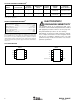
IA
COMMON
(2)
INA326R
1
V
IN−
V
IN+
V
O
Filtered
V
O
6
2
1
8
3
G = 2(R
2
/R
1
)
f
O
= 1kHz
R
O
100Ω
C
O
(1)
1µF
R
2
C
2
(1)
7
+2.5V
4
0.1µF
−2.5V
5
(1) C
2
and C
O
combine to form a 2-pole response that is −3dB at 1kHz.
Each individual pole is at 1.5kHz.
(2) Output voltage is referenced to IA
COMMON
(see text).
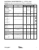
DESIRED R
1
R
2
|| C
2
GAIN (Ω)(Ω|| nF)
0.1 400k 20k || 5
0.2 400k 40k || 2.5
0.5 400k 100k || 1
1 400k 200k || 0.5
2 200k 200k || 0.5
5 80k 200k || 0.5
10 40k 200k || 0.5
20 20k 200k || 0.5
50 8k 200k || 0.5
100 4k 200k || 0.5
200 2k 200k || 0.5
500 2k 500k || 0.2
1000 2k 1M || 0.1
2000 2k 2M || 0.05
5000 2k 5M || 0.02
10000 2k 10M || 0.01
APPLICATIONS INFORMATION
Figure 1 shows the basic connections required for operation of
the INA326. A 0.1µF capacitor, placed close to and across the
power-supply pins is strongly recommended for highest accu-
racy. R
o
C
o
is an output filter that minimizes auto-correction
circuitry noise. This output filter may also serve as an anti-
aliasing filter ahead of an Analog-to-Digital (A/D) converter. It
is also optional based on desired precision.
The output reference terminal is taken at the low side of R
2
(IA
COMMON
).
The INA326 uses a unique internal topology to achieve excel-
lent Common-Mode Rejection (CMR). Unlike conventional
instrumentation amplifiers, CMR is not affected by resistance
in the reference connections or sockets. See “Inside the
INA326” for further detail. To achieve best high-frequency
CMR, minimize capacitance on pins 1 and 8.
FIGURE 1. Basic Connections. NOTE: Connections for INA327 differ—see Pin Configuration for detail.
SETTING THE GAIN
The INA326 is a 2-stage amplifier with each stage gain set
by R
1
and R
2
, respectively (see Figure 5, “Inside the INA326”,
for details). Overall gain is described by the equation:
G
R
R
= 2
2
1
(1)
The stability and temperature drift of the external gain-setting
resistors will affect gain by an amount that can be directly
inferred from the gain equation (1).
Resistor values for commonly used gains are shown in
Figure 1. Gain-set resistor values for best performance are
different for +5V single-supply and for ±2.5V dual-supply
operation. Optimum value for R
1
can be calculated by:
R
1
= V
IN, MAX
/12.5µA (2)
where R
1
must be no less than 2kΩ.
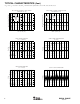
DESIRED R
1
R
2
|| C
2
GAIN (Ω)(Ω|| nF)
0.1 400k 20k || 5
0.2 400k 40k || 2.5
0.5 400k 100k || 1
1 200k 100k || 1
2 100k 100k || 1
5 40k 100k || 1
10 20k 100k || 1
20 10k 100k || 1
50 4k 100k || 1
100 2k 100k || 1
200 2k 200k || 0.5
500 2k 500k || 0.2
1000 2k 1M || 0.1
2000 2k 2M || 0.05
5000 2k 5M || 0.02
10000 2k 10M || 0.01
NOTES: (1) C
2
and C
O
combine to form a 2-pole response that is –3dB at 1kHz. Each individual pole is at 1.5kHz. (2) Output voltage is referenced to
IA
COMMON
(see text). (3) Output offset voltage required for measurement near zero (see Figure 6).
INA326
V
O
Filtered
V
O
6
G = 2(R
2
/R
1
)
f
O
= 1kHz
R
O
100Ω
C
O
(1)
1µF
R
2
C
2
(1)
7
V+
4
0.1µF
5
IA
COMMON
(2)
R
1
(1) C
2
and C
O
combine to form a 2-pole response that is −3dB at 1kHz.
Each individual pole is at 1.5kHz.
(2) Output voltage is referenced to IA
COMMON
(see text).
(3) Output offset voltage required for measurement near zero (see Figure 28).
Single-supply operation may require
R
2
> 100kΩ for full output swing.
This may produce higher input referred
offset voltage. See
Offset Voltage,
Drift, and Circuit Values
for detail.
1
8
V
IN−
V
IN+
2
3
(3)