
Datasheet


INA322
12
SBOS174B
OFFSET VOLTAGE ERROR CALCULATION
The offset voltage (V
OS
) of the INA322EA has a specified
maximum of 10mV with a +5V power supply and the
common-mode voltage at V
S
/2. Additional specifications
for power-supply rejection and common-mode rejection are
provided to allow the user to easily calculate worst-case
expected offset under the conditions of a given application.
Power Supply Rejection Ratio (PSRR) is specified in µV/V.
For the INA322, worst case PSRR is 250µV/V, which
means for each volt of change in power supply, the offset
may shift up to 250µV. Common-Mode Rejection Ratio
(CMRR) is specified in dB, which can be converted to
µV/V using the following equation:
CMRR (in µV/V) = 10
[(CMRR in dB)/–20]
• 10
6
For the INA322, the worst case CMRR over the specified
common-mode range is 60dB (at G = 25) or about
1mV/V This means that for every volt of change in com-
mon-mode, the offset will shift less than 1mV.
These numbers can be used to calculate excursions from the
specified offset voltage under different application condi-
tions. For example, an application might configure the
amplifier with a 3.3V supply with 1V common-mode. This
configuration varies from the specified configuration, repre-
senting a 1.7V variation in power supply (5V in the offset
specification versus 3.3V in the application) and a 0.65V
variation in common-mode voltage from the specified
V
S
/2.
Calculation of the worst-case expected offset would be as
follows:
Adjusted V
OS
= Maximum specified V
OS
+
(power-supply variation) • PSRR +
(common-mode variation) • CMRR
V
OS
= 10mV + (1.7V • 0.250mV/V) + (0.65V • 1mV/V)
= ±11.075mV
However, the typical value will be closer to 2.2mV (calcu-
lated using the typical values).
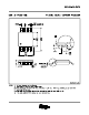
FEEDBACK CAPACITOR IMPROVES RESPONSE
For optimum settling time and stability with high-imped-
ance feedback networks, it may be necessary to add a
feedback capacitor across the feedback resistor, R
F
, as shown
in Figure 8. This capacitor compensates for the zero created
by the feedback network impedance and the INA322’s RG-
pin input capacitance (and any parasitic layout capacitance).
The effect becomes more significant with higher impedance
networks. Also, R
X
and C
L
can be added to reduce high-
frequency noise.
FIGURE 8. Feedback Capacitor Improves Dynamic Perfor-
mance.
It is suggested that a variable capacitor be used for the
feedback capacitor since input capacitance may vary be-
tween instrumentation amplifiers, and layout capacitance is
difficult to determine. For the circuit shown in Figure 8, the
value of the variable feedback capacitor should be chosen by
the following equation:
R
IN
• C
IN
= R
F
• C
F
Where C
IN
is equal to the INA322’s RG-pin input capaci-
tance (typically 3pF) plus the layout capacitance. The ca-
pacitor can be varied until optimum performance is ob-
tained.
INA322
V+
V
OUT
R
IN
R
IN
• C
IN
= R
F
•
C
F
R
F
R
X
C
L
C
IN
Where C
IN
is equal to the INA322’s input capacitance
(approximately 3pF) plus any parastic layout capacitance.
5
3
2
8
7
6
4
1
Shutdown
RG
V
IN
–
V–
V
IN
+
REF
C
F