
Datasheet


Frame 1 SMBus ALERT Response Address Byte Frame 2 Slave Address Byte
(1)
Start By
Master
ACK By
INA230
From
INA230
NACK By
Master
Stop By
Master
1 9 1
9
SDA
SCL
ALERT
0 0 0 1 1 0 0 R/
W 1 0 0 A3 A2 A1 A0 0
Frame 1 Two-Wire Slave Address Byte
(1)
Frame 2 Register Pointer Byte
1
Start By
Master
ACK By
INA230
ACK By
INA230
1 9 1 9
SDA
SCL
0 0 A3 A2 A1 A0 R/
W P7 P6 P5 P4 P3 P2 P1 P0 Stop
¼
INA230
SBOS601 –FEBRUARY 2012
www.ti.com
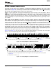
Figure 26 shows the timing diagram for the SMBus alert response operation. Figure 27 illustrates a typical
register pointer configuration.
(1) The value of the slave address byte is determined by the settings of the A0 and A1 pins. Refer to Table 7.
Figure 26. Timing Diagram for SMBus Alert
(1) The value of the slave address byte is determined by the settings of the A0 and A1 pins. Refer to Table 7.
Figure 27. Typical Register Pointer Set
26 Submit Documentation Feedback Copyright © 2012, Texas Instruments Incorporated
Product Folder Link(s): INA230