
Datasheet


INA219
www.ti.com
SBOS448F –AUGUST 2008– REVISED SEPTEMBER 2011
REGISTER INFORMATION
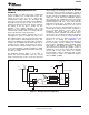
The INA219 uses a bank of registers for holding
Register contents are updated 4μs after completion of
configuration settings, measurement results,
the write command. Therefore, a 4μs delay is
maximum/minimum limits, and status information.
required between completion of a write to a given
Table 4 summarizes the INA219 registers; Figure 12
register and a subsequent read of that register
illustrates registers.
(without changing the pointer) when using SCL
frequencies in excess of 1MHz.
Table 4. Summary of Register Set
POINTER
ADDRESS POWER-ON RESET
HEX REGISTER NAME FUNCTION BINARY HEX TYPE
(1)
All-register reset, settings for bus
00 Configuration Register voltage range, PGA Gain, ADC 00111001 10011111 399F R/W
resolution/averaging.
01 Shunt Voltage Shunt voltage measurement data. Shunt voltage — R
02 Bus Voltage Bus voltage measurement data. Bus voltage — R
03 Power
(2)
Power measurement data. 00000000 00000000 0000 R
Contains the value of the current flowing
04 Current
(2)
00000000 00000000 0000 R
through the shunt resistor.
Sets full-scale range and LSB of current
05 Calibration and power measurements. Overall 00000000 00000000 0000 R/W
system calibration.
(1) Type: R = Read-Only, R/W = Read/Write.
(2) The Power Register and Current Register default to '0' because the Calibration Register defaults to '0', yielding a zero current value until
the Calibration Register is programmed.
Copyright © 2008–2011, Texas Instruments Incorporated Submit Documentation Feedback 25
Product Folder Link(s): INA219