
Datasheet


ADC
Power
Supply
Load
R
SHUNT
C
BYPASS
0.1µF
5V Supply
-
+
IN-
IN+
GND
V+
OUT
REF
Micro-
controller
INA210
,
INA211
,
INA212
,
INA213
,
INA214
,
INA215
www.ti.com
SBOS437F –MAY 2008–REVISED JUNE 2014
8.3 Feature Description
8.3.1 Basic Connections
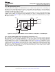
Figure 23 shows the basic connections of the INA210-INA215. The input pins, IN+ and IN–, should be connected
as closely as possible to the shunt resistor to minimize any resistance in series with the shunt resistor.
Figure 23. Typical Application
Power-supply bypass capacitors are required for stability. Applications with noisy or high-impedance power
supplies may require additional decoupling capacitors to reject power-supply noise. Connect bypass capacitors
close to the device pins.
On the RSW package options, two pins are provided for each input. These pins should be tied together (that is,
tie IN+ to IN+ and tie IN– to IN–).
8.3.2 Selecting R
S
The zero-drift offset performance of the INA210-INA215 offers several benefits. Most often, the primary
advantage of the low offset characteristic enables lower full-scale drops across the shunt. For example, non-
zero-drift current shunt monitors typically require a full-scale range of 100 mV.
The INA210-INA215 series gives equivalent accuracy at a full-scale range on the order of 10 mV. This accuracy
reduces shunt dissipation by an order of magnitude with many additional benefits.
Alternatively, there are applications that must measure current over a wide dynamic range that can take
advantage of the low offset on the low end of the measurement. Most often, these applications can use the lower
gains of the INA213, INA214 or INA215 to accommodate larger shunt drops on the upper end of the scale. For
instance, an INA213 operating on a 3.3-V supply could easily handle a full-scale shunt drop of 60 mV, with only
100 μV of offset.
Copyright © 2008–2014, Texas Instruments Incorporated Submit Documentation Feedback 13
Product Folder Links: INA210 INA211 INA212 INA213 INA214 INA215