
Datasheet


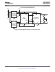


V
(see Note B)
I
1.5 V
CANL
CANH
V
IO
STB
RXD
I
O
C
(see Note A)
L
V
O
V
OL
V
OH
1.5 V
3.5 V
400 mV
t
BUS
0.7 µs
2.65 V
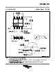
V
I
V
O
CANH
CANL
TXD
STB
V
O(CANH)
V = V + V
SYM O(CANH) O(CANL)
V
O(CANL)
V
I
R
L
SN65HVDA540
SN65HVDA541
www.ti.com
........................................................................................................................................................................................................ SLLS981 – MAY 2009
A. C
L
= 15 pF and includes instrumentation and fixture capacitance within ± 20%.
B. For V
I
bit width ≤ 0.7 µ s, V
O
= V
OH
. For V
I
bit width ≥ 5 µ s, V
O
= V
OL
. V
I
input pulses are supplied from a generator
with the following characteristics: t
r
/t
f
< 6 ns.
Figure 14. t
BUS
Test Circuit and Waveforms
A. All V
I
input pulses are from 0 V to V
IO
and supplied by a generator having the following characteristics: t
r
/t
f
≤ 6 ns,
Pulse Repetition Rate (PRR) = 250 kHz, 50% duty cycle.
Figure 15. Driver Output Symmetry Test Circuit
Copyright © 2009, Texas Instruments Incorporated Submit Documentation Feedback 13
Product Folder Link(s): SN65HVDA540 SN65HVDA541