
Datasheet


DS92LX2121, DS92LX2122
SNLS330I –MAY 2010–REVISED APRIL 2013
www.ti.com
DS92LX2122 Deserializer PIN DESCRIPTIONS (continued)
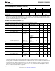
Pin Name Pin No. I/O, Type Description
POWER AND GROUND
SSCG Power, 1.8V ±5%
VDDSSCG 3 Digital Power
Power supply must be connect regardless if SSCG function is in operation
TTL Output Buffer Power, The single-ended outputs and control input are
VDDOR1/2/3 29, 20, 7 Digital Power
powered from V
DDIO
. V
DDIO
can be connected to a 1.8V ±5% or 3.3V ±10%
VDDD 17 Digital Power Digital Core Power, 1.8V ±5%
VDDR 36 Analog Power Rx Analog Power, 1.8V ±5%
VDDCML 40 Analog Power Bi-directional Channel Driver Power, 1.8V ±5%
VDDPLL 45 Analog Power PLL Power, 1.8V ±5%
DAP must be grounded. Connect to the ground plane (GND) with at least 16
VSS DAP Ground, DAP
vias.
These devices have limited built-in ESD protection. The leads should be shorted together or the device placed in conductive foam
during storage or handling to prevent electrostatic damage to the MOS gates.
Absolute Maximum Ratings
(1)(2)
Supply Voltage ( V
DD1V8
) −0.3V to +2.5V
Supply Voltage (V
DD3V3
) −0.3V to +4.0V
LVCMOS Input Voltage (V
DD1V8
) −0.3V to +(V
DD1V8
+ 0.3V)
LVCMOS Input Voltage (V
DD3V3
) −0.3V to +(V
DD3V3
+ 0.3V)
LVCMOS Output Voltage (V
DD
) −0.3V to +(V
DD
+ 0.3V)
CML Receiver Input Voltage (V
DD1V8
) −0.3V to (V
DD1V8
+ 0.3V)
CML Driver Output Voltage (V
DD1V8
) −0.3V to (V
DD1V8
+ 0.3V)
Junction Temperature +150°C
Storage Temperature −65°C to +150°C
Maximum Package Power Dissipation Capacity 1/θ
JA
°C/W above +25°
Package Derating:
DS92LX2121 40L WQFN
θ
JA
(based on 16 thermal vias) 30.7 °C/W
θ
JC
(based on 16 thermal vias) 6.8 °C/W
DS92LX2122 48L WQFN
θ
JA
(based on 16 thermal vias) 26.9 °C/W
θ
JC
(based on 16 thermal vias) 4.4 °C/W
ESD Rating (IEC61000–4–2) R
D
= 330Ω, C
S
= 150 pF
Air Discharge (DOUT+, DOUT-, RIN+, RIN-) ≥±25 kV
Contact Discharge (DOUT+, DOUT-, RIN+, RIN-) ≥±10 kV
ESD Rating (HBM) ≥±8 kV
For soldering specifications, see the Absolute Maximum Ratings for Soldering Application Report (literature number SNOA549).
(1) “Absolute Maximum Ratings” indicate limits beyond which damage to the device may occur, including inoperability and degradation of
device reliability and/or performance. Functional operation of the device and/or non-degradation at the Absolute Maximum Ratings or
other conditions beyond those indicated in the Recommended Operating Conditions is not implied. The Recommended Operating
Conditions indicate conditions at which the device is functional; the device should not be operated beyond such conditions.
(2) If Military/Aerospace specified devices are required, please contact the Texas Instruments Sales Office/ Distributors for availability and
specifications.
Recommended Operating Conditions
Min Nom Max Units
V
DD
(1.8V) 1.71 1.8 1.89 V
V
DDIO
(1.8V Mode) 1.71 1.8 1.89 V
V
DDIO
(3.3V Mode) 3 3.3 3.6 V
6 Submit Documentation Feedback Copyright © 2010–2013, Texas Instruments Incorporated
Product Folder Links: DS92LX2121 DS92LX2122