
Datasheet


DS92LX2121, DS92LX2122
www.ti.com
SNLS330I –MAY 2010–REVISED APRIL 2013
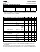
DS92LX2122 Deserializer PIN DESCRIPTIONS
Pin Name Pin No. I/O, Type Description
LVCMOS PARALLEL INTERFACE
ROUT[20:0] 5, 6, 8, 9, 10, Outputs, LVCMOS Parallel data outputs.
11, 12, 13, 14,
15, 16, 18, 19,
21, 22, 23, 24,
25, 26, 27, 28
Pixel Clock Output Pin.
PCLK 4 Output, LVCMOS Strobe edge set by RFB configuration. In SLEEP, outputs are controlled by the
OSS_SEL.
General Purpose Input (GPI)
General-purpose pins individually configured as inputs; which are used to
GPI[3:0] 30, 31, 32, 33 Input/Output, Digital
control and respond to various commands.
SERIAL CONTROL BUS - I
2
C COMPATIBLE
Input/Output, Open Clock line for the serial control bus communication
SCL 2
Drain SCL requires an external pull-up resistor to V
DDIO
.
Input/Output, Open Data line for serial control bus communication
SDA 1
Drain SDA requires an external pull-up resistor to V
DDIO
.
I
2
C Mode Select
M/S = L, Master; device generates and drives the SCL clock line. Device is
Input, LVCMOS w/ connected to slave peripheral on teh bus.
M/S 47
pull up
M/S = H, Slave (default); device accepts SCL clock input and is attached to an
I
2
C controller master on the bus. Slave mode does not generate the SCL clock,
but uses the clock generated by teh Master for teh data transfer.
Continuous Address Decoder
Input pin to select the Slave Device Address.
CAD 48 Input, analog
Input is connect to external resistor divider to programmable Device ID address
(see Serial Control Bus Connection)
CONTROL AND CONFIGURATION
Power down Mode Input Pin.
PDB = H, Receiver is enabled and is ON.
Input, LVCMOS w/
PDB 35
PDB = L, Receiver is in Sleep (Power down mode). When the Receiver is in the
pull down
SLEEP state, the LVCMOS Outputs are in TRI-STATE, the PLL is shutdown
and IDD is minimized.
LOCK Status Output Pin.
LOCK = H, PLL is Locked, outputs are active
LOCK 34 Output, LVCMOS
LOCK = L, PLL is unlocked, ROUT and PCLK output states are controlled by
OSS_SEL. May be used as Link Status.
Reserved.
Pin 43: Leave pin open.
RES 38, 39, 43, 46 -
Pin 46: This pin MUST be tied LOW.
Pins 38, 39: Route to test point as differential pair or leave open if unused.
BIST MODE
BIST Enable Pin.
Input, LVCMOS w/
BISTEN 44 BISTEN = H, BIST Mode is enabled.
pull down
BISTEN = L, BIST Mode is disabled.
PASS Output Pin for BIST mode.
PASS = H, ERROR FREE Transmission
PASS 37 Output, LVCOMS
PASS = L, one or more errors were detected in the received payload.
Leave Open if unused. Route to test point (pad) recommended.
Channel Link III INTERFACE
Non-inverting differential input, back channel output. The interconnect must be
RIN+ 41 Input/Output, CML
AC coupled with a 0.1μF capacitor.
Inverting differential input, back channel output. The interconnect must be AC
RIN- 42 Input/Output, CML
coupled with a 0.1 μF capacitor.
Copyright © 2010–2013, Texas Instruments Incorporated Submit Documentation Feedback 5
Product Folder Links: DS92LX2121 DS92LX2122