
Datasheet


DS92LX2121, DS92LX2122
SNLS330I –MAY 2010–REVISED APRIL 2013
www.ti.com
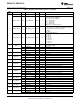
Table 1. DS92LX2121 Control Registers (continued)
Addr
Name Bits Field R/W Default Description
(Hex)
Reserved 7:3 RESERVED 0 Reserved.
1: Valid PCLK detected
PCLK Detect 2 PCLK DETECT R 0
0: Valid PCLK not detected
C
Reserved 1 RESERVED Reserved.
Cable Link Detect 0: Cable link not detected
0 LINK DETECT R 0
Status 1: Cable link detected
D Reserved 7:0 RESERVED Reserved.
E Reserved 7:0 RESERVED Reserved.
F Reserved 7:0 RESERVED Reserved.
10 Reserved 7:0 RESERVED Reserved.
11 Reserved 7:0 RESERVED Reserved.
12 Reserved 7:0 RESERVED Reserved.
GPCR[7] 0: LOW
GPCR[6] 1: HIGH
GPCR[5]
GPCR[4]
General Purpose
13 7:0 RW 0
Control Reg
GPCR[3]
GPCR[2]
GPCR[1]
GPCR[0]
Table 2. DS92LX2122 Control Registers
Addr
Name Bits Field R/W Default Description
(Hex)
7-bit address of Deserializer;
7:1 DEVICE ID RW 0x60h 0x60h
(1100_000X) default
0 I
2
C Device ID
0: Device ID is from CAD
0 DES ID RW 0
1: Register I
2
C Device ID overrides CAD
7:3 RESERVED Reserved
Remote Wake-up Select
1: Enable. Generate remote wakeup signal automatically
2 REM_WAKEUP RW 0
wake-up the Serializer in Standby mode
1 Reset
0: Disable. Puts the Serializer in Standby mode
1: Resets the device to default register values. Does not
1 DIGITALRESET0 RW 0 self clear
affect device I
2
C Bus or Device ID
0 DIGITALRESET1 RW 0 self clear 1: Digital Reset, retained register value
18 Submit Documentation Feedback Copyright © 2010–2013, Texas Instruments Incorporated
Product Folder Links: DS92LX2121 DS92LX2122