
Datasheet


DS92LX1621, DS92LX1622
SNLS327I –MAY 2010–REVISED JANUARY 2014
www.ti.com
DS92LX1622 Deserializer PIN DESCRIPTIONS (continued)
Pin Name Pin No. I/O, Type Description
Input/Output, Open Data line for serial control bus communication
SDA 2
Drain SDA requires an external pull-up resistor to V
DDIO
.
I
2
C Mode Select
Input, LVCMOS w/
M/S 40 M/S = L, Master; device generates and drives the SCL clock line
pull up
M/S = H, Slave (default); device accepts SCL clock input
Continuous Address Decoder
Input pin to select the Slave Device Address.
CAD 1 Input, analog
Input is connect to external resistor divider to programmable Device ID address
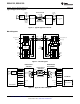
(See Figure 29)
CONTROL AND CONFIGURATION
Power down Mode Input Pin.
PDB = H, Receiver is enabled and is ON.
Input, LVCMOS w/
PDB 29
PDB = L, Receiver is in Sleep (Power down mode). When the Receiver is in the
pull down
SLEEP state, the LVCMOS Outputs are in TRI-STATE, the PLL is shutdown
and IDD is minimized.
LOCK Status Output Pin.
LOCK = H, PLL is Locked, outputs are active
LOCK 28 Output, LVCMOS
LOCK = L, PLL is unlocked, ROUT and PCLK output states are controlled by
OSS_SEL. May be used as Link Status.
When BISTEN = L; Normal operation
PASS 31 Output, LVCMOS PASS is high to indicate no errors are detected. The PASS pin asserts low to
indicate a CRC error was detected on the link.
Reserved.
RES 32, 33, 39 - Pin 39: This pin MUST be tied LOW.
Pins 32, 33: Leave pin open.
BIST MODE
BIST Enable Pin.
Input, LVCMOS w/
BISTEN 37 BISTEN = H, BIST Mode is enabled.
pull down
BISTEN = L, BIST Mode is disabled.
PASS Output Pin for BIST mode.
PASS = H, ERROR FREE Transmission
PASS 31 Output, LVCMOS
PASS = L, one or more errors were detected in the received payload.
Leave Open if unused. Route to test point (pad) recommended.
Channel Link III INTERFACE
RIN+ 35 Input/Output, CML Noninverting differential input, back channel output.
RIN- 36 Input/Output, CML Inverting differential input, back channel output.
POWER AND GROUND
SSCG Power, 1.8V ±5%
VDDSSCG 4 Digital Power
Power supply must be connect regardless if SSCG function is in operation
TTL Output Buffer Power, The single-ended outputs and control input are
VDDOR1/2/3 25, 16, 8 Digital Power
powered from V
DDIO
. V
DDIO
can be connected to a 1.8V ±5% or 3.3V ±10%
VDDD 13 Digital Power Digital Core Power, 1.8V ±5%
VDDR 30 Analog Power Rx Analog Power, 1.8V ±5%
VDDCML 34 Analog Power Bi-Directional Control Channel Driver Power, 1.8V ±5%
VDDPLL 38 Analog Power PLL Power, 1.8V ±5%
VSS DAP Ground DAP must be grounded. Connect to the ground plane with at least 16 vias.
These devices have limited built-in ESD protection. The leads should be shorted together or the device placed in conductive foam
during storage or handling to prevent electrostatic damage to the MOS gates.
6 Submit Documentation Feedback Copyright © 2010–2014, Texas Instruments Incorporated
Product Folder Links: DS92LX1621 DS92LX1622