
Datasheet


64
REN
63
V
DD
62
V
SS
61
V
DD
60
V
SS
59
RRFB
58
R
IN
-
57
R
IN
+
56
55
54
53
17
18
19
20
21
22
23
24
25
26
27
28
R
OUT
[15]
R
OUT
[14]
R
OUT
[13]
R
OUT
[12]
LOCK
RCLK
V
SS
V
DD
R
OUT
[11]
R
OUT
[10]
R
OUT
[9]
R
OUT
[8]
12
R
OUT
[16]
11
R
OUT
[17]
10
R
OUT
[18]
9
R
OUT
[19]
8
V
SS
7
V
DD
6
R
OUT
[20]
5
R
OUT
[21]
4
R
OUT
[22]
3
R
OUT
[23]
2RES0
1
37
38
39
40
41
42
43
44
45
46
47
48
R
OUT
[7]
R
OUT
[6]
R
OUT
[5]
R
OUT
[4]
V
SS
V
DD
R
OUT
[3]
R
OUT
[2]
R
OUT
[1]
R
OUT
[0]
V
SS
V
DD
PTO GROUP 3
PTO GROUP 1
PTO GROUP 2
16
15
14
13
33
34
35
36
RES0
52
51
50
49
29
30
31
32
DS90UR124
RES0
RES0
RES0
RES0
RES0
RES0
RES0
V
SS
V
DD
RES0
PASS
RPWDNB
BISTEN
BISTM
RAOFF
SLEW
V
SS
V
DD
RES0
PTOSEL
DS90UR124Q, DS90UR241Q
SNLS231N –SEPTEMBER 2006–REVISED MARCH 2013
www.ti.com
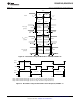
DS90UR124 Pin Diagram
Figure 19. Deserializer - DS90UR124
TOP VIEW
DS90UR124 Deserializer Pin Descriptions
Pin # Pin Name I/O/PWR Description
LVCMOS PARALLEL INTERFACE PINS
35-38, R
OUT
[7:0] LVCMOS_O Receiver Parallel Interface Data Outputs – Group 1
41-44
19-22, R
OUT
[15:8] LVCMOS_O Receiver Parallel Interface Data Outputs – Group 2
27-30
7-10, R
OUT
[23:16] LVCMOS_O Receiver Parallel Interface Data Outputs – Group 3
13-16
24 RCLK LVCMOS_O Parallel Interface Clock Output Pin. Strobe edge set by RRFB configuration pin.
CONTROL AND CONFIGURATION PINS
55 RRFB LVCMOS_I Receiver Clock Edge Select Pin
RRFB = H; R
OUT
LVCMOS Outputs strobed on the Rising Clock Edge.
RRFB = L; R
OUT
LVCMOS Outputs strobed on the Falling Clock Edge.
60 REN LVCMOS_I Receiver Data Enable
REN = H; R
OUT
[23-0] and RCLK are Enabled (ON).
REN = L; R
OUT
[23-0] and RCLK are Disabled (OFF), Receiver R
OUT
[23-0] and RCLK Outputs are
in TRI-STATE, PLL still operational and locked to TCLK.
48 RPWDNB LVCMOS_I Receiver Power Down Bar
RPWDNB = H; Receiver is Enabled and ON
RPWDNB = L; Receiver is in power down mode (Sleep), R
OUT
[23-0], RCLK, and LOCK are in
TRI-STATE stand-by mode, PLL is shutdown to minimize power consumption.
49 PTOSEL LVCMOS_I Progressive Turn On Operation Selection
PTO = H; R
OUT
[23:0] are grouped into three groups of eight, with each group switching about ±1
UI to ±2 UI apart relative to RCLK. (Figure 15)
PTO = L; PTO Spread Mode, R
OUT
[23:0] outputs are spread ±1 UI to ±2 UI and RCLK spread ±1
UI. (Figure 16) See Applications Informations section for more details.
16 Submit Documentation Feedback Copyright © 2006–2013, Texas Instruments Incorporated
Product Folder Links: DS90UR124Q DS90UR241Q