
Datasheet


DS90LV048A
SNLS045B –JULY 1999–REVISED APRIL 2013
www.ti.com
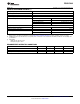
ELECTRICAL CHARACTERISTICS
Over Supply Voltage and Operating Temperature ranges, unless otherwise specified.
(1)(2)
Symbol Parameter Conditions Pin Min Typ Max Units
V
TH
Differential Input High Threshold V
CM
= +1.2V, 0.05V, 2.95V
(3)
R
IN+
, −35 0 mV
R
IN−
V
TL
Differential Input Low Threshold −100 −35 mV
VCMR Common-Mode Voltage Range VID = 200mV pk to pk
(4)
0.1 2.3 V
I
IN
Input Current V
IN
= +2.8V V
CC
= 3.6V or 0V −10 ±5 +10 μA
V
IN
= 0V −10 ±1 +10 μA
V
IN
= +3.6V V
CC
= 0V -20 ±1 +20 μA
V
OH
Output High Voltage I
OH
= −0.4 mA, V
ID
= +200 mV R
OUT
2.7 3.3 V
I
OH
= −0.4 mA, Input terminated 2.7 3.3 V
I
OH
= −0.4 mA, Input shorted 2.7 3.3 V
V
OL
Output Low Voltage I
OL
= 2 mA, V
ID
= −200 mV 0.05 0.25 V
I
OS
Output Short Circuit Current Enabled, V
OUT
= 0V
(5)
−15 −47 −100 mA
I
OZ
Output TRI-STATE Current Disabled, V
OUT
= 0V or V
CC
−10 ±1 +10 μA
V
IH
Input High Voltage EN, 2.0 V
CC
V
EN*
V
IL
Input Low Voltage GND 0.8 V
I
I
Input Current V
IN
= 0V or V
CC
, Other Input = V
CC
or GND −10 ±5 +10 μA
V
CL
Input Clamp Voltage I
CL
= −18 mA −1.5 −0.8 V
I
CC
No Load Supply Current EN = V
CC
, Inputs Open V
CC
9 15 mA
Receivers Enabled
I
CCZ
No Load Supply Current EN = GND, Inputs Open
1 5 mA
Receivers Disabled
(1) Current into device pins is defined as positive. Current out of device pins is defined as negative. All voltages are referenced to ground
unless otherwise specified.
(2) All typicals are given for: V
CC
= +3.3V, T
A
= +25°C.
(3) V
CC
is always higher than R
IN+
and R
IN−
voltage. R
IN−
and R
IN+
are allowed to have a voltage range −0.2V to V
CC
− VID/2. However, to
be compliant with AC specifications, the common voltage range is 0.1V to 2.3V
(4) The VCMR range is reduced for larger VID. Example: if VID = 400mV, the VCMR is 0.2V to 2.2V. The fail-safe condition with inputs
shorted is not supported over the common-mode range of 0V to 2.4V, but is supported only with inputs shorted and no external
common-mode voltage applied. A VID up to V
CC
− 0V may be applied to the R
IN+
/ R
IN−
inputs with the Common-Mode voltage set to
V
CC
/2. Propagation delay and Differential Pulse skew decrease when VID is increased from 200mV to 400mV. Skew specifications
apply for 200mV ≤ VID ≤ 800mV over the common-mode range .
(5) Output short circuit current (I
OS
) is specified as magnitude only, minus sign indicates direction only. Only one output should be shorted
at a time, do not exceed maximum junction temperature specification.
4 Submit Documentation Feedback Copyright © 1999–2013, Texas Instruments Incorporated
Product Folder Links: DS90LV048A