Datasheet
Table Of Contents

DS90CR217
www.ti.com
SNLS226A –OCTOBER 2006–REVISED FEBRUARY 2013
The high-speed transport of LVDS signals has been demonstrated on several types of cables with excellent
results. However, the best overall performance has been seen when using Twin-Coax cable. Twin-Coax has very
low cable skew and EMI due to its construction and double shielding. All of the design considerations discussed
here and listed in the supplemental application notes provide the subsystem communications designer with many
useful guidelines. It is recommended that the designer assess the tradeoffs of each application thoroughly to
arrive at a reliable and economical cable solution.
BOARD LAYOUT
To obtain the maximum benefit from the noise and EMI reductions of LVDS, attention should be paid to the
layout of differential lines. Lines of a differential pair should always be adjacent to eliminate noise interference
from other signals and take full advantage of the noise canceling of the differential signals. The board designer
should also try to maintain equal length on signal traces for a given differential pair. As with any high-speed
design, the impedance discontinuities should be limited (reduce the numbers of vias and no 90 degree angles on
traces). Any discontinuities which do occur on one signal line should be mirrored in the other line of the
differential pair. Care should be taken to ensure that the differential trace impedance match the differential
impedance of the selected physical media (this impedance should also match the value of the termination
resistor that is connected across the differential pair at the receiver's input). Finally, the location of the CHANNEL
LINK TxOUT pins should be as close as possible to the board edge so as to eliminate excessive pcb runs. All of
these considerations will limit reflections and crosstalk which adversely effect high frequency performance and
EMI.
UNUSED INPUTS
All unused inputs at the TxIN inputs of the transmitter may be tied to ground or left no connect.
TERMINATION
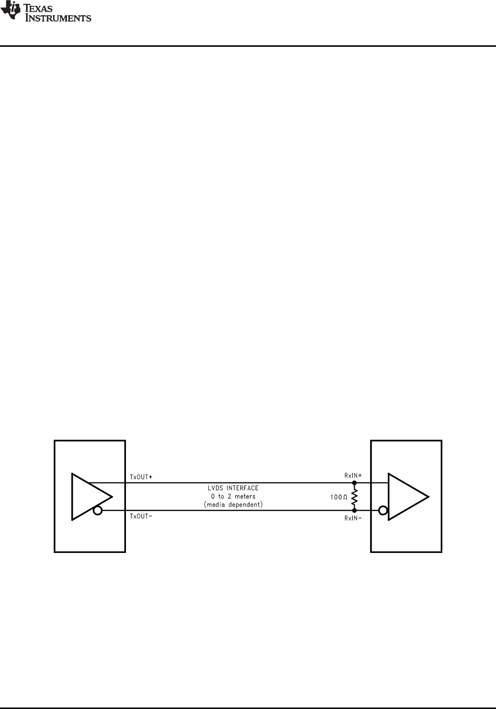
Use of current mode drivers requires a terminating resistor across the receiver inputs. The CHANNEL LINK
chipset will normally require a single 100Ω resistor between the true and complement lines on each differential
pair of the receiver input. The actual value of the termination resistor should be selected to match the differential
mode characteristic impedance (90Ω to 120Ω typical) of the cable. Figure 13 shows an example. No additional
pull-up or pull-down resistors are necessary as with some other differential technologies such as PECL. Surface
mount resistors are recommended to avoid the additional inductance that accompanies leaded resistors. These
resistors should be placed as close as possible to the receiver input pins to reduce stubs and effectively
terminate the differential lines.
Figure 13. LVDS Serialized Link Termination
DECOUPLING CAPACITORS
Bypassing capacitors are needed to reduce the impact of switching noise which could limit performance. For a
conservative approach three parallel-connected decoupling capacitors (Multi-Layered Ceramic type in surface
mount form factor) between each V
CC
and the ground plane(s) are recommended. The three capacitor values are
0.1 μF, 0.01 μF and 0.001 μF. An example is shown in Figure 14. The designer should employ wide traces for
power and ground and ensure each capacitor has its own via to the ground plane. If board space is limiting the
number of bypass capacitors, the PLL V
CC
should receive the most filtering/bypassing. Next would be the LVDS
V
CC
pins and finally the logic V
CC
pins.
Copyright © 2006–2013, Texas Instruments Incorporated Submit Documentation Feedback 9
Product Folder Links: DS90CR217


