
Datasheet


DS90C363, DS90CF364
SNLS123C –SEPTEMBER 1999–REVISED APRIL 2013
www.ti.com
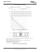
AC Timing Diagrams (continued)
Figure 6. DS90C363 (Transmitter) LVDS Output Load and Transition Times
Figure 7. DS90CF364 (Receiver) CMOS/TTL Output Load and Transition Times
Figure 8. DS90C363 (Transmitter) Input Clock Transition Time
Measurements at Vdiff=0V
TCCS measured between earliest and latest LVDS edges
TxCLK Differential Low → High Edge
Figure 9. DS90C363 (Transmitter) Channel-to-Channel Skew
Figure 10. DS90C363 (Transmitter) Setup/Hold and High/Low Times
6 Submit Documentation Feedback Copyright © 1999–2013, Texas Instruments Incorporated
Product Folder Links: DS90C363 DS90CF364