
Datasheet


f
f / 16
f / 8
f / 4
f / 2
Steady State, Low
Steady State, Low
f / 16
f / 8
f / 4
f / 2
Steady State, Low
Steady State, Low
f / 16
f / 8
f / 4
f / 2
Steady State, Low
Steady State, Low
Steady State, High
Steady State, High
Steady State, High
TxCLK IN / RxCLK OUT
TxIN0 / RxOUT0
TxIN1 / RxOUT1
TxIN2 / RxOUT2
TxIN3 / RxOUT3
TxIN4 / RxOUT4
TxIN5 / RxOUT5
TxIN6 / RxOUT6
TxIN7 / RxOUT7
TxIN8 / RxOUT8
TxIN9 / RxOUT9
TxIN10 / RxOUT10
TxIN11 / RxOUT11
TxIN12 / RxOUT12
TxIN13 / RxOUT13
TxIN14 / RxOUT14
TxIN15 / RxOUT15
TxIN16 / RxOUT16
TxIN17 / RxOUT17
TxIN18 / RxOUT18
TxIN19 / RxOUT19
TxIN20 / RxOUT20
Dot Clk
R0
R1
R2
R3
R4
R5
G0
G1
G2
G3
G4
G5
B0
B1
B2
B3
B4
B5
HSYNC
VSYNC
ENA
Device Pin Name
Signal Signal Pattern Signal Frequency
DS90CF364A, DS90CF384A
SNLS040I –JUNE 2000–REVISED APRIL 2013
www.ti.com
(1) The worst case test pattern produces a maximum toggling of digital circuits, LVDS I/O and CMOS/TTL I/O.
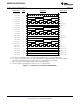
(2) The 16 grayscale test pattern tests device power consumption for a “typical” LCD display pattern. The test pattern
approximates signal switching needed to produce groups of 16 vertical stripes across the display.
(3) Figure 3 and Figure 5 show a falling edge data strobe (TxCLK IN/RxCLK OUT).
(4) Recommended pin to signal mapping. Customer may choose to define differently.
Figure 5. “16 Grayscale” Test Pattern (DS90CF364A)
6 Submit Documentation Feedback Copyright © 2000–2013, Texas Instruments Incorporated
Product Folder Links: DS90CF364A DS90CF384A