
Datasheet


DS90C365A
SNLS181I –APRIL 2004–REVISED APRIL 2013
www.ti.com
These devices have limited built-in ESD protection. The leads should be shorted together or the device placed in conductive foam
during storage or handling to prevent electrostatic damage to the MOS gates.
Absolute Maximum Ratings
(1)
Supply Voltage (V
CC
) −0.3V to +4V
CMOS/TTL Input Voltage −0.5V to (V
CC
+ 0.3)V
LVDS Driver Output Voltage −0.3V to (V
CC
+ 0.3)V
LVDS Output Short Circuit Duration Continuous
Junction Temperature +150°C
Storage Temperature −65°C to +150°C
Lead Temperature (Soldering, 4 seconds) +260°C
Maximum Package Power Dissipation Capacity at 25°C, TSSOP Package 1.98W
Package Derating 16 mW/°C above +25°C
HBM, 1.5kΩ, 100pF 7kV
ESD Rating
EIAJ, 0Ω, 200 pF 500V
Latch Up Tolerance at 25°C ±100mA
(1) “Absolute Maximum Ratings” are those values beyond which the safety of the device cannot be verified. They are not meant to imply
that the device should be operated at these limits. The tables of “Electrical Characteristics” specify conditions for device operation.
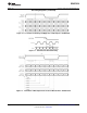
Recommended Operating Conditions
Min Nom Max Unit
Supply Voltage (V
CC
) 3.0 3.3 3.6 V
Operating Free Air Temperature (T
A
) −10 +25 +70 °C
Supply Noise Voltage (V
CC
) 200 mV
PP
TxCLKIN frequency 18 85 MHz
Electrical Characteristics
(1)
Over recommended operating supply and temperature ranges unless otherwise specified.
Symbol Parameter Conditions Min Typ
(2)
Max Unit
LVCMOS/LVTTL DC SPECIFICATIONS
V
IH
High Level Input Voltage 2.0 V
CC
V
V
IL
Low Level Input Voltage 0 0.8 V
V
CL
Input Clamp Voltage I
CL
= −18 mA −0.79 −1.5 V
I
IN
Input Current V
IN
= 0.4V, 2.5V or V
CC
+1.8 +10 μA
V
IN
= GND −10 0 μA
LVDS DC SPECIFICATIONS
V
OD
Differential Output Voltage R
L
= 100Ω 250 345 450 mV
ΔV
OD
Change in V
OD
between 35 mV
complimentary output states
V
OS
Offset Voltage
(3)
1.13 1.25 1.38 V
ΔV
OS
Change in V
OS
between 35 mV
complimentary output states
I
OS
Output Short Circuit Current V
OUT
= 0V, R
L
= 100Ω −3.5 −5 mA
I
OZ
Output TRI-STATE
®
Current Power Down = 0V, ±1 ±10 μA
V
OUT
= 0V or V
CC
(1) Current into device pins is defined as positive. Current out of device pins is defined as negative. Voltages are referenced to ground
unless otherwise specified (except V
OD
and ΔV
OD
).
(2) Typical values are given for V
CC
= 3.3V and T
A
= +25°C unless specified otherwise.
(3) V
OS
previously referred as V
CM
.
2 Submit Documentation Feedback Copyright © 2004–2013, Texas Instruments Incorporated
Product Folder Links: DS90C365A