
Datasheet


EQ
IN+
IN-
PE
VCC
OUT+
OUT-
NC
1
2
3
4
8
6
5
7
GND
DAP
PE
OUT+
OUT-
EQ
IN+
IN-
DS25BR100
SNLS217F –MARCH 2007–REVISED APRIL 2013
www.ti.com
Device Information
Device Function Termination Option Available Signal Conditioning
DS25BR100 Buffer / Repeater Internal 100Ω for LVDS inputs 2 Levels: PE and EQ
DS25BR101 Buffer / Repeater External termination required 2 Levels: PE and EQ
DS25BR110 Receiver Internal 100Ω for LVDS inputs 4 Levels: EQ
DS25BR120 Driver Internal 100Ω for LVDS inputs 4 Levels: PE
DS25BR150 Buffer / Repeater Internal 100Ω for LVDS inputs None
Block Diagram
DS25BR101 eliminates 100Ω input termination.
Pin Diagram
PIN DESCRIPTIONS
Pin Name Pin Name Pin Type Pin Description
EQ 1 Input Equalizer select pin.
IN+ 2 Input Non-inverting LVDS input pin.
IN- 3 Input Inverting LVDS input pin.
PE 4 Input Pre-emphasis select pin.
NC 5 NA "NO CONNECT" pin.
OUT- 6 Output Inverting LVDS output pin.
OUT+ 7 Output Non-inverting LVDS Output pin.
VCC 8 Power Power supply pin.
GND DAP Power Ground pad (DAP - die attach pad).
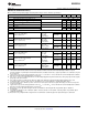
Control Pins (PE and EQ) Truth Table
EQ PE Equalization Level Pre-emphasis Level
0 0 Low (Approx. 4 dB at 1.56 GHz) Off
0 1 Low (Approx. 4 dB at 1.56 GHz) Medium (Approx. 6 dB at 1.56 GHz)
1 0 Medium (Approx. 8 dB at 1.56 GHz) Off
1 1 Medium (Approx. 8 dB at 1.56 GHz) Medium (Approx. 6 dB at 1.56 GHz)
2 Submit Documentation Feedback Copyright © 2007–2013, Texas Instruments Incorporated
Product Folder Links: DS25BR100