
Datasheet


DS100BR410
www.ti.com
SNLS326B –OCTOBER 2010–REVISED APRIL 2013
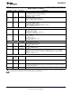
Electrical Characteristics (continued)
Over recommended operating supply and temperature ranges with default register settings unless other specified.
(1)
Parameter Test Conditions Min Typ Max Units
I
IN-P
Input Leakage Current with Internal V
IN
= V
DD
, with internal pull-down +65 μA
Pull-Down/Up Resistors resistors
V
IN
= GND, with internal pull-up -50 μA
resistors
Signal Detect
SDH Signal Detect ON Threshold Level Default input signal level to assert 130 mV
p-p
SD pin, 10.3125 Gbps
SDL Signal Detect OFF Threshold Level Default input signal level to de- 60 mV
p-p
assert SD, 10.3125 Gbps
CML Receiver Inputs (IN_n+, IN_n-)
V
TX
Source Transmit Launch Signal AC-Coupled Requirement,
Level (IN diff) Differential measurement at point 600 1600 mV
P-P
A. Figure 1
R
LI
Differential Input Return Loss - 100 MHz – 6 GHz, with fixture’s
-15 dB
SDD11 effect de-embedded
CML Driver Outputs (OUT_n+, OUT_n-)
V
OD
Output Differential Voltage Level
(3)
, Differential measurement with
Figure 2 OUT+ and OUT- terminated by
50Ω to GND, AC-Coupled, 750 970 1150 mV
P-P
VOD_SEL = open (1.0 Vp-p),
DE_SEL = GND
Differential measurement with
OUT+ and OUT- terminated by
50Ω to GND, AC-Coupled, 1140 mV
P-P
VOD_SEL = V
DD
(1.2 Vp-p),
DE_SEL = GND
V
OD_DE
De-Emphasis Levels
(4) (5)
DE_SEL = 20kΩ to GND,
-3 dB
VOD_SEL = V
DD
(1.2 Vp-p)
DE_SEL = open,
-6 dB
VOD_SEL = V
DD
(1.2 Vp-p)
DE_SEL = V
DD
,
-9 dB
VOD_SEL = V
DD
(1.2 Vp-p)
t
R
, t
F
Transition Time 20% to 80% of differential output
voltage, measured within 1” from 30 38 45 ps
output pins. Figure 2
R
LO
Differential Output Return Loss - 100 MHz – 6 GHz, with fixture’s
SDD22 effect de-embedded. IN+ = static -15 dB
high.
t
PLHD
Differential Low to High Propagation delay measurement at
240 ps
Propagation Delay 50% crossing between input to
output, 100 Mbps. Figure 3
t
PHLD
Differential High to Low
240 ps
Propagation Delay
t
CCSK
Inter Pair Channel to Channel Difference in 50% crossing
7 ps
Skew between channels
t
PPSK
Part to Part Output Skew Difference in 50% crossing
20 ps
between outputs
RJ Random Jitter V
TX
= 1.0 Vp-p, BST_[2:0] = 000,
0.3 ps
rms
(4) (6)
(3) Measured with clock-like {11111 00000} pattern.
(4) Measured with clock-like {11111 00000} pattern.
(5) The de-emphasis level of −3 dB, −6 dB, −9 dB are for V
OD
= 1.2 Vp-p. At lower V
OD
level, the de-emphasis levels are reduced.
(6) Random jitter contributed by the equalizer is defined as sqrt (J
OUT
2
– J
IN
2
). J
OUT
is the random jitter at equalizer outputs in ps-rms, see
point C of Figure 1; J
IN
is the random jitter at the input of the equalizer in ps-rms, see point B of Figure 1.
Copyright © 2010–2013, Texas Instruments Incorporated Submit Documentation Feedback 5
Product Folder Links: DS100BR410