
Datasheet


DS100BR410
SNLS326B –OCTOBER 2010–REVISED APRIL 2013
www.ti.com
Absolute Maximum Ratings
(1)
Supply Voltage (V
DD
) -0.5V to +2.75V
2.5 I/O Voltage -0.5V to +2.75V
(LVCMOS and Analog Input)
3.3 LVCMOS I/O Voltage -0.5V to +4.0V
(SDA, SDC, CS)
CML Input Voltage (IN_n+/-) -0.5V to +2.75V
CML Output Voltage (OUT_n+/-) -0.5V to +2.75V
Junction Temperature +150°C
Storage Temperature -65°C to +150°C
ESD Rating HBM, STD - JESD22-A114F ≥7 kV
MM, STD - JESD22-A115-A ≥200 V
CDM, STD - JESD22-C101-D ≥1250 V
Thermal Resistance
θ
JA
, No Airflow,
4 layer JEDEC, 9 thermal vias 27.6 °C/W
For soldering specifications: see product folder at www.ti.com
http://www.ti.com/lit/SNOA549
(1) “Absolute Maximum Ratings” indicate limits beyond which damage to the device may occur, including inoperability and degradation of
device reliability and/or performance. Functional operation of the device and/or non-degradation at the Absolute Maximum Ratings or
other conditions beyond those indicated in the Recommended Operating Conditions is not implied.
Recommended Operating Conditions
(1)
Min Typ Max Units
Supply Voltage
V
DD
to GND 2.375 2.5 2.625 V
Ambient Temperature -40 25 +85 °C
(1) The Recommended Operating Conditions indicate conditions at which the device is functional and the device should not be operated
beyond such conditions.
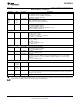
Electrical Characteristics
Over recommended operating supply and temperature ranges with default register settings unless other specified.
(1)
Parameter Test Conditions Min Typ Max Units
POWER
PD Power Supply Consumption Device Output Enabled
(EN[3:0] = High), 220 275 mW
VOD_SEL = open (1.0 Vp-p)
Device Output Disable
25 40 mW
(EN[3:0] = Low)
PS
NT
Supply Noise Tolerance
(2)
50 Hz to 100 Hz 100 mV
P-P
100 Hz to 10 MHz 40 mV
P-P
10 MHz to 5.0 GHz 10 mV
P-P
2.5 LVCMOS DC Specifications
V
IH
High Level Input Voltage 1.75 V
DD
V
V
IL
Low Level Input Voltage -0.3 0.7 V
V
OH
High Level Output Voltage I
OH
= -3mA 2.0 V
V
OL
Low Level Output Voltage I
OL
= 3mA 0.4 V
I
IN
Input Leakage Current V
IN
= V
DD
+10 μA
V
IN
= GND -10 μA
(1) Typical values represent most likely parametric norms at V
DD
= 2.5V, T
A
= 25°C., and at the Recommended Operation Conditions at the
time of product characterization and are not ensured.
(2) Specification is ensured by characterization at optimal boost setting and is not tested in production.
4 Submit Documentation Feedback Copyright © 2010–2013, Texas Instruments Incorporated
Product Folder Links: DS100BR410