
Datasheet


1
2
3
4
5
6
7
8
9
10
11
12
13
14
15
16
17
18
19
20
21
22
23
24
36
35
34
33
32
31
30
29
28
27
26
25
48
47
46
45
44
43
42
41
40
39
38
37
IN_3-
IN_3+
IN_2-
IN_2+
IN_1-
IN_1+
IN_0-
IN_0+
OUT_3-
OUT_3+
OUT_2-
OUT_2+
OUT_1-
OUT_1+
OUT_0-
OUT_0+
V
DD
V
DD
V
DD
V
DD
GND
GND
GND
GND
V
DD
V
DD
GND
GND
BST_1
BST_0
CS
SDC
SDA
OOB_DIS
V
DD
SD0
EN0
SD1
EN1
SD2
EN2
SD3
EN3
RES
BST_2
VOD_SEL
DE_SEL
PIN_MODE
DS100BR410
TOP VIEW
DAP = GND
DS100BR410
SNLS326B –OCTOBER 2010–REVISED APRIL 2013
www.ti.com
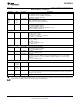
Connection Diagram
Pin Descriptions
Pin Name Pin # I/O, Type
(1)
Description
HIGH SPEED DIFFERENTIAL I/O
IN_0+ 1 I, CML Inverting and non-inverting CML differential inputs to the equalizer. An on-chip 100Ω
IN_0– 2 terminating resistor connects IN_0+ to IN_0-.
IN_1+ 4 I, CML Inverting and non-inverting CML differential inputs to the equalizer. An on-chip 100Ω
IN_1– 5 terminating resistor connects IN_1+ to IN_1-.
IN_2+ 8 I, CML Inverting and non-inverting CML differential inputs to the equalizer. An on-chip 100Ω
IN_2– 9 terminating resistor connects IN_2+ to IN_2-.
IN_3+ 11 I, CML Inverting and non-inverting CML differential inputs to the equalizer. An on-chip 100Ω
IN_3– 12 terminating resistor connects IN_3+ to IN_3-.
OUT_0+ 36 O, CML Inverting and non-inverting CML differential outputs from the driver. An on-chip 100Ω
OUT_0– 35 terminating resistor connects OUT_0+ to OUT_0-.
OUT_1+ 33 O, CML Inverting and non-inverting CML differential outputs from the driver. An on-chip 100Ω
OUT_1– 32 terminating resistor connects OUT_1+ to OUT_1-.
OUT_2+ 29 O, CML Inverting and non-inverting CML differential outputs from the driver. An on-chip 100Ω
OUT_2– 28 terminating resistor connects OUT_2+ to OUT_2-.
OUT_3+ 26 O, CML Inverting and non-inverting CML differential outputs from the driver. An on-chip 100Ω
OUT_3– 25 terminating resistor connects OUT_3+ to OUT_3-.
2.5V LVCMOS CONTROL PINS
BST_2 37 I, LVCMOS BST_2, BST_1, and BST_0 select the equalizer boost level for all channels.
BST_1 14 BST_2 and BST_1 are internally pulled high.
BST_0 23 BST_0 is internally pulled low. See Table 1
EN0 44 I, LVCMOS Enable channel n input.
EN1 42 When held High, normal operation is selected.
EN2 40 When held Low, standby mode is selected.
EN3 38 EN is internally pulled High.
(1) Note: I = Input O = Output, LVCMOS pins are 2.5 V levels only, only SMBus pins SDA, SDC and CS are 3.3V tolerant.
2 Submit Documentation Feedback Copyright © 2010–2013, Texas Instruments Incorporated
Product Folder Links: DS100BR410