
Datasheet


DRV8412
DRV8432
www.ti.com
SLES242C –DECEMBER 2009–REVISED MAY 2010
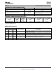
ELECTRICAL CHARACTERISTICS
T
A
= 25 °C, PVDD = 50 V, GVDD = VDD = 12 V, f
Sw
= 400 kHz, unless otherwise noted. All performance is in accordance
with recommended operating conditions unless otherwise specified.
PARAMETER TEST CONDITIONS MIN TYP MAX UNIT
Internal Voltage Regulator and Current Consumption
V
REG
Voltage regulator, only used as a reference node VDD = 12 V 2.95 3.3 3.65 V
Idle, reset mode 9 12 mA
I
VDD
VDD supply current
Operating, 50% duty cycle 10.5
Reset mode 1.7 2.5 mA
I
GVDD_X
Gate supply current per half-bridge
Operating, 50% duty cycle 8
I
PVDD_X
Half-bridge X (A, B, C, or D) idle current Reset mode 0.7 1 mA
Output Stage
MOSFET drain-to-source resistance, low side (LS) T
J
= 25°C, GVDD = 12 V 80 mΩ
R
DS(on)
MOSFET drain-to-source resistance, high side (HS) T
J
= 25°C, GVDD = 12 V 80 mΩ
V
F
Diode forward voltage drop T
J
= 25°C - 125°C, I
O
= 5 A 1 V
t
R
Output rise time Resistive load, I
O
= 5 A 14 nS
t
F
Output fall time Resistive load, I
O
= 5 A 14 nS
t
PD_ON
Propagation delay when FET is on Resistive load, I
O
= 5 A 38 nS
t
PD_OFF
Propagation delay when FET is off Resistive load, I
O
= 5 A 38 nS
t
DT
Dead time between HS and LS FETs Resistive load, I
O
= 5 A 5.5 nS
I/O Protection
Gate supply voltage GVDD_X undervoltage
V
uvp,G
8.5 V
protection threshold
V
uvp,hyst
(1)
Hysteresis for gate supply undervoltage event 0.8 V
OTW
(1)
Overtemperature warning 115 125 135 °C
OTW
hyst
(1)
Hysteresis temperature to reset OTW event 25 °C
OTSD
(1)
Overtemperature shut down 150 °C
OTE- OTE-OTW overtemperature detect temperature
25 °C
OTW
differential
(1)
difference
Hysteresis temperature for FAULT to be released
OTSD
HYST
(1)
25 °C
following an OTSD event
I
OC
Overcurrent limit protection Resistor—programmable, nominal, R
OCP
= 27 kΩ 9.7 A
Time from application of short condition to Hi-Z of
I
OCT
Overcurrent response time 250 ns
affected FET(s)
Internal pulldown resistor at the output of each Connected when RESET_AB or RESET_CD is
R
PD
1 kΩ
half-bridge active to provide bootstrap capacitor charge
Static Digital Specifications
V
IH
High-level input voltage PWM_A, PWM_B, PWM_C, PWM_D, M1, M2, M3 2 3.6 V
V
IH
High-level input voltage RESET_AB, RESET_CD 2 5.5 V
PWM_A, PWM_B, PWM_C, PWM_D, M1, M2, M3,
V
IL
Low-level input voltage 0.8 V
RESET_AB, RESET_CD
l
lkg
Input leakage current –100 100 mA
OTW / FAULT
Internal pullup resistance, OTW to VREG, FAULT to
R
INT_PU
20 26 35 kΩ
VREG
Internal pullup resistor only 2.95 3.3 3.65
V
OH
High-level output voltage V
External pullup of 4.7 kΩ to 5 V 4.5 5
V
OL
Low-level output voltage I
O
= 4 mA 0.2 0.4 V
(1) Specified by design
Copyright © 2009–2010, Texas Instruments Incorporated Submit Documentation Feedback 7
Product Folder Link(s): DRV8412 DRV8432